- FIBER OPTIC TRANSCEIVERS >40G & 25G Transceivers >40G QSFP+ SR4 MPO 150 m
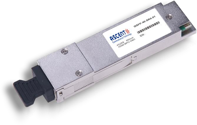
40G QSFP+ SR4 MPO 150 m
Ascent’s QSFP-40-SR4-01 QSFP transceivers are designed for use in 40 Gigabit per second links over multimode fiber. They are compliant with the QSFP+ MSA and IEEE 802.3ba-2010 40GBASE-SR4. The optical transmitter portion of the transceiver incorporates a 4-channel VCSEL array, a 4-channel input buffer and laser driver, diagnostic monitors, control and bias blocks. For module control, the control interface incorporates a Two Wire Serial interface of clock and data signals. Diagnostic monitors for VCSEL bias, module temperature, transmitted optical power, received optical power and supply voltage are implemented and results are available through the TWS interface. Alarm and warning thresholds are established for the monitored attributes. Fault detection or channel deactivation through the TWS interface will disable the channel. Status, alarm/warning and fault information are available via the TWS interface. The optical receiver portion of the transceiver incorporates a 4-channel PIN photodiode array, a 4- channel TIA array, a 4-channel output buffer, diagnostic monitors, and control and bias blocks. Diagnostic monitors for optical input power are implemented and results are available through the TWS interface. Alarm and warning thresholds are established for the monitored attributes.
· Compliant with QSFP+ MSA Specification
· 4x10Gbps 850nm VCSEL-based Transmitter
· Maximum Link Length of 150m Via OM3 Multimode Fiber(MMF)
· Wide Operating Temperature: 0°C to +70°C
· RoHS and FCC compliant
Absolute Maximum Ratings
Parameter | Symbol | Min. | Max. | Unit | Note |
Storage Temperature | Tstorage | -40 | +85 | °C | |
Relative Humidity | RH | 0 | +85 | % |
Recommended Operating Conditions
Parameter | Symbol | Min. | Typ. | Max. | Unit | Note |
Operating Case Temperature | TC | 0 | 70 | °C | ||
Power Supply Voltage | Vcc | 3.135 | 3.3 | 3.465 | V | |
Signaling Rate each Channel | 10.3125 | Gbps | ||||
Supply Noise Rejection | --- | --- | 100 | mV | ||
Receiver Differential Data Output | --- | 100 | Ohm | |||
Operating Distance | D | 150 | m | @ OM3 MMF |
Optical Characteristics(T=25°C, unless note)
Parameter | Symbol | Min. | Typ. | Max. | Unit | Note |
Transmitter | ||||||
Signaling Rate, each Lane (Range) | GBb | 10.3125 | GBb | |||
Center Wavelength | λ | 840 | 850 | 860 | nm | |
RMS Spectral Width | SW | 0.6 | nm | |||
Average Launch Power, each Lane | Pf | -8.4 | 2.4 | dBm | ||
Optical Modulation Amplitude (OMA), each Lane | TxOMA | -6.4 | 3 | dBm | ||
Average Launch Power of OFF Transmitter, each Lane | -30 | dBm | ||||
Extinction Ratio | ER | 3 | dB | |||
Optical Return Loss Tolerance | 12 | dB | ||||
Reciever | ||||||
Signaling Rate, each Lane (Range) | GBb | 10.3125 | GBb | |||
Center Wavelength | λ | 840 | 860 | nm | ||
Damage Threshold | 3.4 | dBm | ||||
Average Power at Receiver Input, each Lane | -10.3 | 2.4 | dBm | |||
Receiver Power Overload | 2.4 | dBm | ||||
Receive Power, each Lane (OMA) | 3 | dBm | ||||
Receiver Sensitivity (OMA) | SOMA | -11.1 | dBm | BER@1e-12 | ||
Receiver Reflectance | -12 | dB | ||||
LOS Assert | LOSA | -30 | dBm | |||
LOS De-Assert | LOSD | -11 | dBm | |||
LOS Hysteresis | 0.5 | dB | ||||
Electrical Characteristics
Parameter | Symbol | Min | Typ. | Max | Unit | Note |
Power Consumption | P | 3.5 | W | |||
Supply Current | Icc | 1050 | mA |
Digital Diagnostic Function
ASCENT’s QSFP-40-SR4-01 supports the 2-wire serial communication protocol as defined in the QSFP+ MSA, which allows real-time access to the following operating parameters:
· Transceiver temperature
· Laser bias current
· Transmitted optical power
· Received optical power
· Transceiver supply voltage
It also access and monitor module information (ex: Media type, Vendor name, Part Number, Serial Number, Wavelength, Voltage, temperature, etc), provides a sophisticated system of alarm and warning flags, which may be used to alert end-users when particular operating parameters are outside of a factory-set normal range.
The operating and diagnostics information is monitored and reported by a Digital Diagnostics Transceiver Controller inside the transceiver, which is accessed through the 2-wire serial interface. When the serial protocol is activated, the serial clock signal (SCL pin) is generated by the host. The positive edge clocks data into the QSFP+ transceiver into those segments of its memory map that are not write-protected. The negative edge clocks data from the QSFP+ transceiver. The serial data signal (SDA pin) is bi-directional for serial data transfer. The host uses SDA in conjunction with SCL to mark the start and end of serial protocol activation. The memories are organized as a series of 8-bit data words that can be addressed individually or sequentially. The 2-wire serial interface provides sequential or random access to the 8 bit parameters, addressed from 00h to the maximum address of the memory.
This clause defines the Memory Map for QSFP+ transceiver used for serial ID, digital monitoring and certain control functions. The interface is mandatory for all QSFP+ devices. The memory map has been changed in order to accommodate 4 optical channels and limit the required memory space. The structure of the memory is shown in below figure-QSFP+ Memory Map. The memory space is arranged into a lower, single page, address space of 128 bytes and multiple upper address space pages. This structure permits timely access to addresses in the lower page, e.g. Interrupt Flags and Monitors. Less time critical entries, e.g. serial ID. information and threshold settings, are available with the Page Select function. The structure also provides address expansion by adding additional upper pages as needed. For example, in below figure upper pages 01 and 02 are optional. Upper page 01 allows implementation of Application Select Table, and upper page 02 provides user read/write space. The lower page and upper pages 00 and 03 are always implemented. The interface address used is A0xh and is mainly used for time critical data like interrupt handling in order to enable a “one-time-read” for all data related to an interrupt situation. After an Interrupt, IntL, has been asserted, the host can read out the flag field to determine the effected channel and type of flag.
For more detailed information including memory map definitions, please see the QSFP+ MSA Specification.
Parameter | Accuracy | Unit |
Internally Measured Transceiver Temperature | +/-3 | °C |
Internally Measured Transceiver Supply Voltage | +/-3 | % |
Measured Tx Bias Current | +/-10 | % |
Measured Tx Output Power | +/-3 | dB |
Measured Rx Received Average Optical Power | +/-3 | dB |

64G SFP56 850nm 100m
64 Gb/s SFP56 SW Fibre Channel 850nm Transceiver
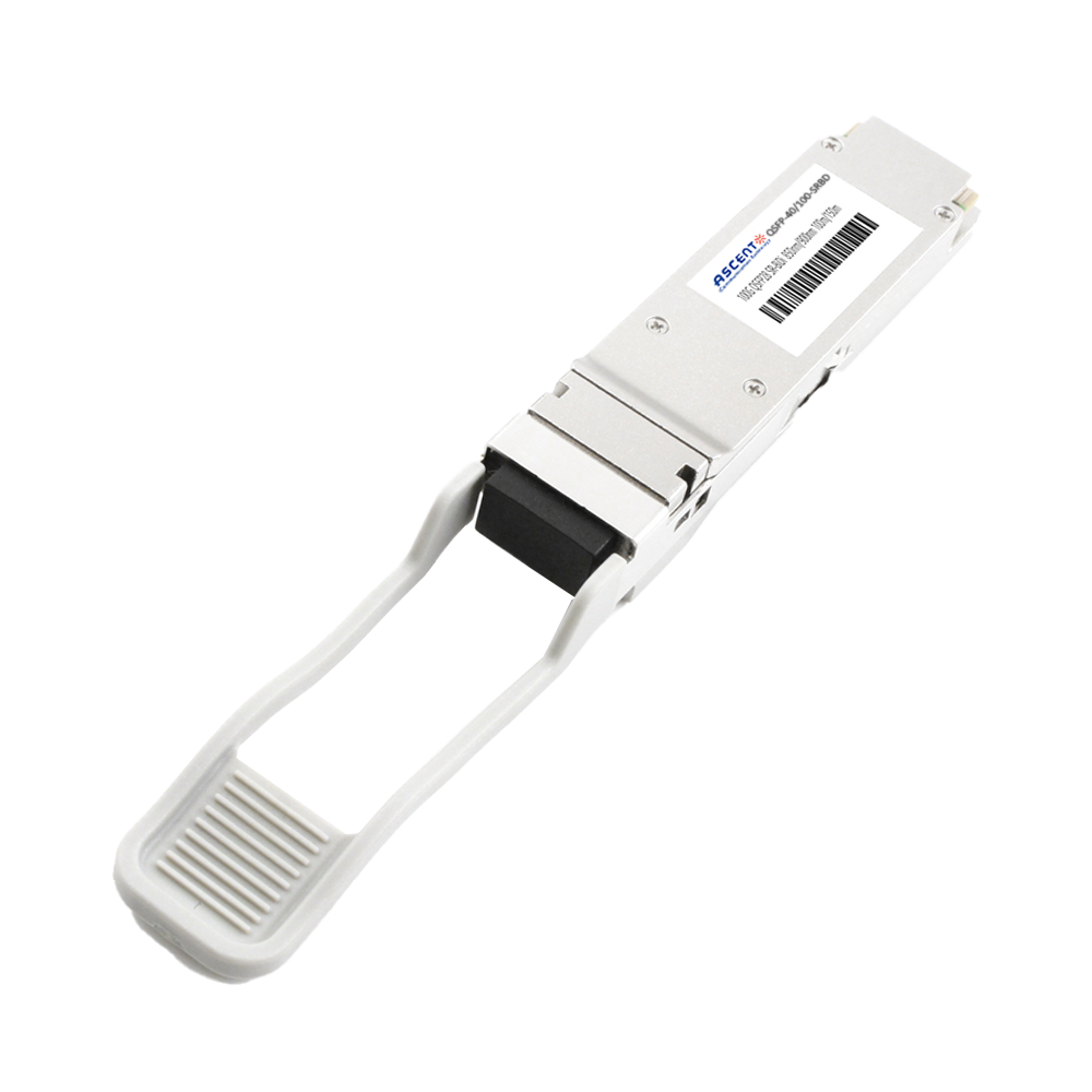
40/100G SFP28 SWDM4 100m
40/100Gb/s QSFP28, Bi-Di, Duplex LC 100m Transceiver

40G QSFP+ ER4 Industrial 40 km
40 Gb/s QSFP+ ER4 40 km Transceiver

40G QSFP+ ER4 40 km
40 Gb/s QSFP+ ER4 40 km Transceiver

40G QSFP+ LR4 Industrial 10 km
40 Gb/s QSFP+ LR4 10 km Transceiver

40G QSFP+ LR4 10 km
QSFP-AQ-LP-W4-10 40 Gb/s QSFP LR4 10 km Transceiver

40G QSFP+ PSM4 2 km
40 Gb/s QSFP+ PSM4 Transceiver 2km
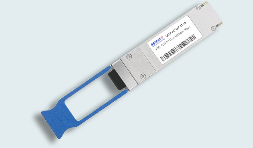
40G QSFP+ PLR4 1310 nm 10 km
QSFP-AQ-MP-31-10 40 Gb/s QSFP+ PSM 1310nm 10km MPO Optical Transceiver
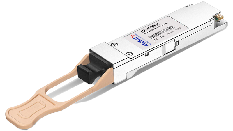
40G QSFP+ CSR4 300m
40 Gb/s 300m QSFP+ CSR4 Transceiver
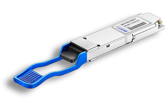
40GBASE-UNIV QSFP+ MMF and SMF
40G QSFP+ UNIV MMF/SMF 150m/2km
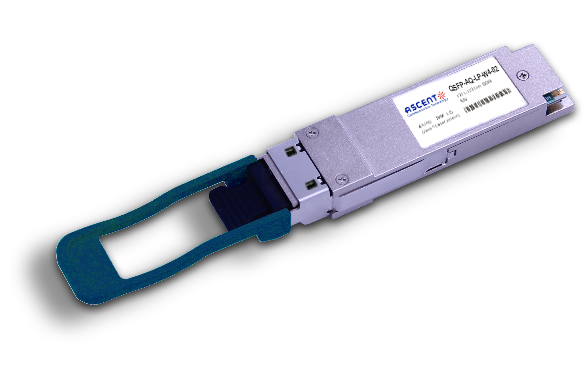
40G QSFP+ CWDM 2 km
40G QSFP+ CWDM 2 km
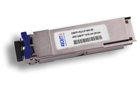
40G QSFP CWDM 20 km
QSFP-AQ-LP-W4-20 40 Gb/s QSFP CWDM 20 km Transceiver
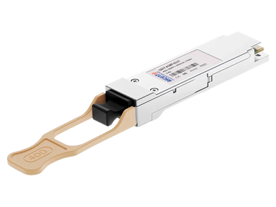
40G QSFP+ SR4 150 m
40 Gb/s 150m QSFP+ SR4 Transceiver with DDM

40G QSFP+ BIDI 150m
40 Gb/s QSFP+ BiDi Transceiver 150m
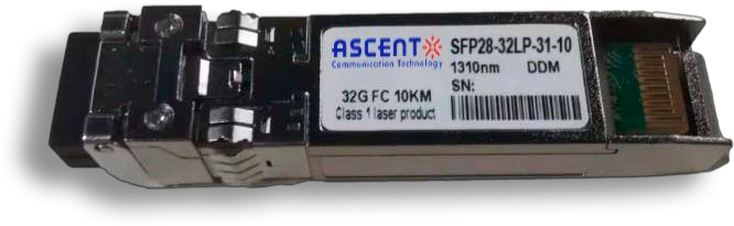
32G SFP28 1310 nm 10 km
32G FC 1310 nm 10 km SFP28 Transceiver

32G SFP28 SR 850 nm 100 m
SFP28-32LP-85-01 32GBASE-SR SFP28 850 nm 100 m DOM Transceiver
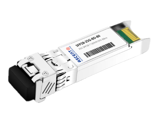
25G SFP28 BIDI 80 km
25G SFP28 BIDI 80 km Transceiver
.png)
25G SFP28 CWDM 10 km(E)
25 Gb/s CWDM EML SFP28 10 km Transceiver
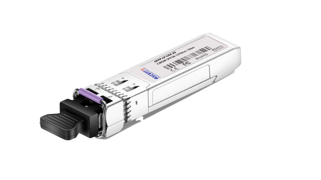
25G SFP28 CWDM 10 km(D)
25 Gb/s CWDM SFP28 10 km Transceiver

25G SFP28 ZR 1310nm 80km
25 Gbps 1310 nm 80 km SFP28 ZR Transceiver
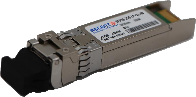
25G SFP28 1310 nm 40km
25 Gb/s 1310 nm Single-Mode SFP28 Transceiver
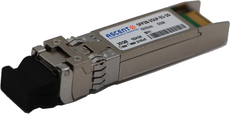
25G SFP28 1310 nm 10 km
SFP28-25LP-31-10 25 Gb/s 1310 nm Single-Mode SFP+ Transceiver
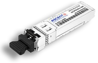
25G SFP28 850 nm 300m
25 Gb/s 850 nm Multi-Mode SFP28 300m Transceiver

25G SFP28 850 nm 100m
SFP28-25LP-85-01 28 Gb/s 850 nm Multi-Mode SFP28 Transceiver

10/25G SFP28 1310nm 40km
10/25 Gb/s SFP28 1310 nm 40km Transceiver

10/25G SFP28 1310nm 10km
10/25 Gb/s SFP28 1310 nm 10km DDM Transceiver

10/25G SFP28 850 nm 300m
10/25 Gb/s SFP28 850 nm 300m Transceiver

10/25G SFP28 850 nm 100m
10/25 Gb/s SFP28 850 nm 100m Transceiver
White Paper
Press Releases
Briefings 1
Briefings 2
Videos, etc.
QRG
Manual1
Manual2
Get in touch with our experts
Feedback