- FIBER OPTIC TRANSCEIVERS >800G & 400G Transceivers >800G OSFP SR8 850 nm 100 m

800G OSFP SR8 850 nm 100 m
Ascentãs OSFP-800G-SR8D-01 is an Eight-Channel, Parallel, Pluggable, Fiber-Optic OSFP for 800 Gigabit Ethernet applications. This transceiver is a high performance module for short-range data communication and interconnect application. The 800GBASE-SR8 OSFP Optical Transceiver Module is designed for use in 800Gb/s systems throughput up to 30m over OM3 or 50m over OM4 multimode fiber (MMF) using a wavelength of 850nm via dual MTP/MPO-12 connectors. Digital diagnostics functions are also available via the I2C interface, as specified by the OSFP MSA, to allow access to real time operating parameters. With these features, this easy to install, hot swappable transceiver is suitable to be used in various applications, such as data centers, high-performance computing networks, enterprise core and distribution layer applications.
OSFP Serial Optical Interface:
ôñ 8x100G PAM4 retimed 800GAUI-8 electrical interface
ôñ Dual MPO- 12 APC connector is provided
ôñ 8 channel VCSEL arrays and 8 channels PIN photo detector arrays
ôñ Maximum link length of 30m on OM3 or 50m on OM4
OSFP MSA Compliant:
ôñ Hot Pluggable OSFP form factor
ôñ Compliant to OSFP Module Specification Rev 5.0
ôñ Compliant with CMIS 5.2
Support Protocol:
ôñ Compliant with IEEE 802.3db
ôñ Compliant to IEEE 802.3ck
Low Power Consumption:
ôñ Less than 14W in temperature range of 0 to 70ô¯C
Absolute Maximum Rating
Parameter | Symbol | Min. | Max. | Unit |
Storage Temperature | Ts | -40 | 85 | ô¯C |
Case Operating Temperature | Top | 0 | 70 | ô¯C |
Relative Humidity (non-condensation) | RH | 15 | 85 | % |
Supply Voltage | Vcc | -0.5 | 3.6 | V |
Receiver Damage Threshold, per Lane | PRdmg | 5 | dBm |
Recommended Operating Conditions
Parameter | Symbol | Min. | Max. | Unit | Notes |
Operating Case Temperature | Top | 0 | 70 | ô¯C | Operating Case Temperature |
Relative Humidity(non-condensing) | RH | 15 | 85 | % | Relative Humidity(non-condensing) |
Power Supply Voltage | Vcc | 3.135 | 3.465 | V | Power Supply Voltage |
Total Power Consumption | Pc | - | 14 | W | Total Power Consumption |
Supply Current per End | 4.465 | A | Supply Current per end | ||
Bit Rate | BR | 850 | Gbps | Bit Rate | |
Fiber Length on OM3 MMF | 30 | m | Fiber Length on OM3 MMF | ||
Fiber Length on OM4 MMF | 50 | m | Fiber Length on OM4 MMF | ||
I2C Clock Frequency | 0 | 400 | kHz | I2C Clock Frequency |
Notes:
1. Under condition of 3.465V operating supply voltage, and 70ô¯C case temperature.
Optical Transmitter
Unless otherwise stated, the following characteristics are defined under recommended operating conditions.
Parameter | Symbol | Min | Typ | Max | Unit | Notes |
Data Rate per Lane | DR | 53.125 | GBd | |||
Modulation Format | PAM4 | |||||
Center Wavelength 1 | ö£ | 840 | 860 | 868 | nm | |
RMS Spectral Width | ü | 0.6 | nm | |||
Average Launch Power, each lane | Pavg | -4.6 | 4 | dBm | ||
Optical Power OMA, each Laneÿ¥max | POMA | 3.5 | dBm | |||
OMAouter, each Lane Min | POMA | max [-2.6 , max(TECQ,TECQ)ã 4.4] | dBm | 3 | ||
Transmitter and Dispersion Eye Closure (TDECQ), each Lane | TDECQ | 4.4 | dB | |||
Transmitter Eye Closure for PAM4 (TECQ), each Lane | TECQ | 4.4 | dB | |||
Extinction Ratio | ER | 2.5 | dB | |||
Transmitter Power Excursion, each Lane | 2.3 | dBm | ||||
Optical Return Loss Tolerance | ORLT | 14 | dB | |||
Optical Power for TX DISABLE | -30 | dBm | ||||
Encircled Fluxb2 | ãË86% at 19 um ãÊ30% at 4.5 um | |||||
Notes:
1. Defined according to the performance of the laser used.
2. Measured into type A1a.2 or type A1a.3, or A1a.4, 50 um fiber, in accordance with IEC 61280-1-4.
3. Max (TECQ, TDECQ)<1.8 dB and 1.8 < max (TECQ, TDECQ) < 4.4 dB
Optical Receiver
Parameter | Symbol | Min. | Typ. | Max. | Unit |
Data Rate per Lane | BR | 53.125 | Gbd | ||
Modulation Format | PAM4 | ||||
Center Wavelength | ö£ | 842 | 850 | 948 | nm |
Damage Threshold | 5 | dBm | |||
Average Receive Power, each Lane | ã6.4 | 4 | dBm | ||
Receive Power, each Lane (OMAouter) | 3.5 | dBm | |||
Receiver Reflectance | Rr | ã 15 | dB | ||
Receiver Sensitivity, each Lane1 | RS = max (-4.6 , TECQ - 6.4) | dBm | |||
Stressed Receiver Sensitivity, each Lane | -2 | dBm | |||
Rx LOS | Assert | -15 | dBm | ||
De-assert | -7.5 | dBm | |||
Hysteresis | 0.5 | 5 | dB | ||
Notes:
1. Receiver sensitivity is informative and is defined for a transmitter with a value of TECQ. Measured with conformance test signal at TP3 for BER = 2.4E-4 Pre-FEC.
Electrical Specification
Parameter | Min. | Typ. | Max. | Unit |
Pre FEC Bit Error Ratio | 2.4E-4 | |||
Post FEC Bit Error Ratio | 1E-12 | |||
Transmitter (each Lane) | ||||
Differential Pk-Pk Input Voltage tolerance | 750 | mV | ||
Differential Termination Mismatch | 10 | % | ||
Eye Height | 10 | mV | ||
Common-Mode to Differential-Mode Return Loss | IEEE802.3ck Equation (120G-1) | dB | ||
Vertical Eye Closure | dB | |||
Effective Return Loss | 7.3 | dB | ||
Transition Time | 10 | ps | ||
Receiver (each Lane) | ||||
Differential Data Output Swing | 300 | 900 | mVpp | |
Differential Termination Mismatch | 10 | % | ||
Eye Height | 15 | mV | ||
Vertical Eye Closure | 12 | dB | ||
Common-Mode to Differential-Mode Return Loss | IEEE802.3ck Equation (120G-1) | |||
Effective Return Loss | 8.5 | dB | ||
Transition Time | 8.5 | ps | ||
Laser Safety
The OSFP-800G-SR8D-01 are Class 1 Laser products according to FDA/CDRH, IEC-60825-1 and IEC60825-2 standards. They must be operated under the specified operating conditions.
Electromagnetic Compatibility
The OSFP-800G-SR8D-01 are designed to meet FCC Class B limits.

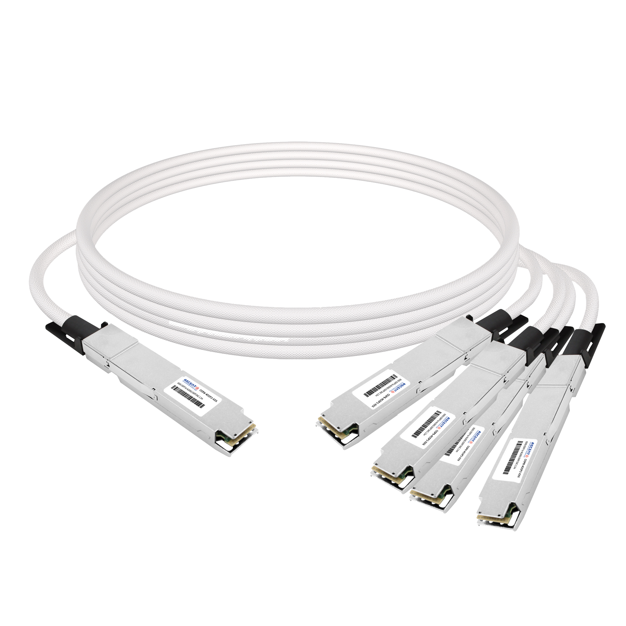
800G OSFP DAC Cable
800G IB NDR OSFP to 4xOSFP RHS Hairtail+ Direct Attach Copper Cable
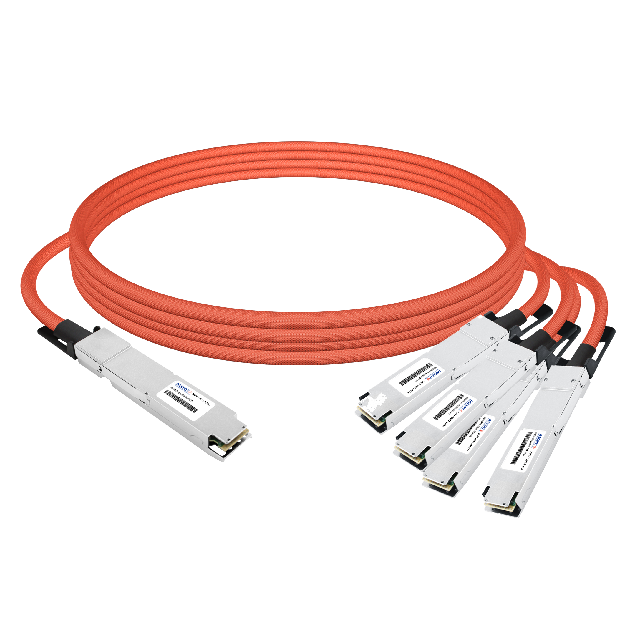
800G OSFP ACC Cable
800G OSFP Breakout to 4x200G OSFP Active Copper Cable

800G OSFP DR8 1310 nm 500 m
800 Gb/s DR8 OSFP 500m Optical Transceiver
400G QSFP56-DD 10km
400G QSFP-DD 4X100G LR1 Optical Transceiver

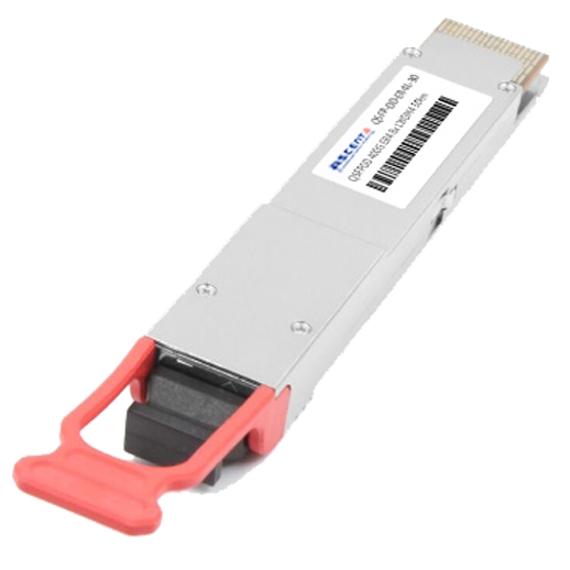
400G QSFP-DD ZR+
QSFP-DD-ZR-80 400 Gb/s QSFP-DD 80 km Transceiver
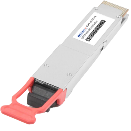
400G QSFP-DD ER8 40 km
QSFP-DD-ER8-40 400 Gb/s QSFP-DD 40 km Transceiver
400G QSFP-DD 30 km
400 Gb/s QSFP-DD 30 km Transceiver
400G QSFP-DD 40 km
400 Gb/s QSFP-DD 40 km Transceiver
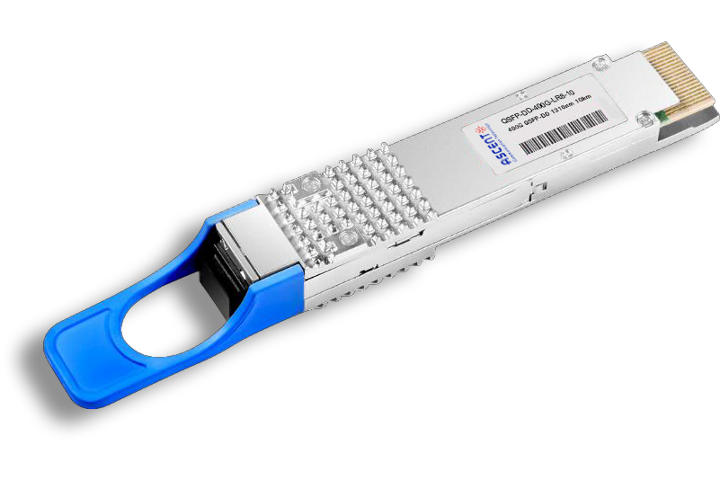
400G QSFP-DD LR8 1310 nm 10 km
QSFP-DD-LR8-10 400 Gb/s QSFP-DD LR8 10 km Transceiver

400G QSFP-DD LR4 CWDM 10 km
QSFP-DD-LR4-10 400 Gb/s QSFP-DD LR4 CWDM 10 km Transceiver
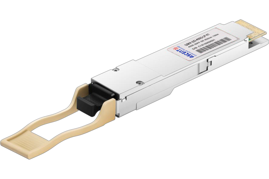
400G QSFP-DD SR8 850 nm 100 m
QSFP-DD-LP-01 400 Gb/s QSFP-DD SR8 100 m Transceiver
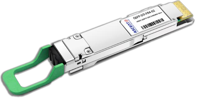
400G QSFP-DD FR4 2km
400 Gb/s QSFP-DD FR4 2 km DDM Transceiver

400G QSFP-DD DR4 500m
400 Gb/s QSFP-DD DR4 500m Transceiver

400G QSFP-DD DCO ZR
400G QSFP-DD DCO ZR Coherent Optical Transceiver

4X100G QSFP-DD LR4 10km
QDD 4x100G 1310nm LR 10 km Transceiver
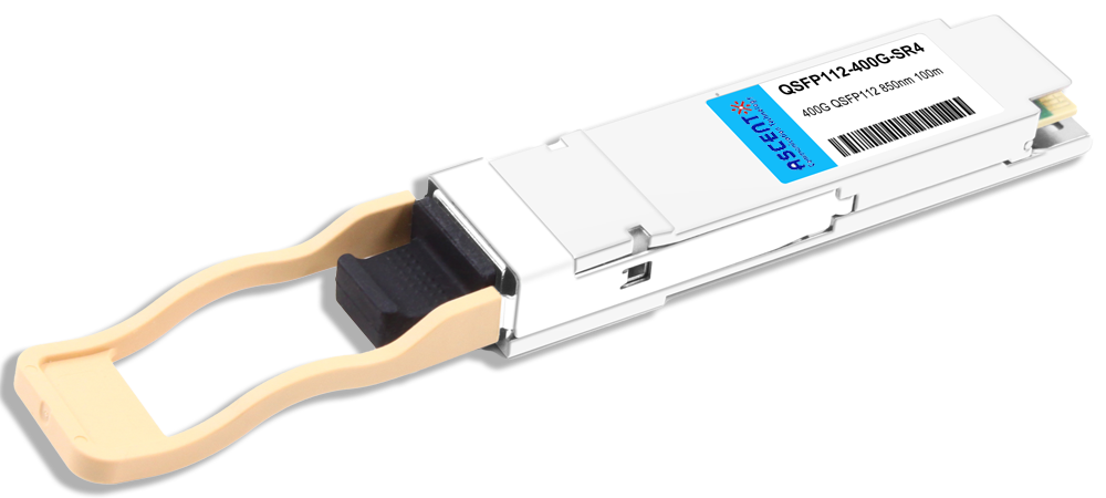
400G QSFP112 SR4 850 nm 100 m
QSFP112-400G-SR4-01 400 Gb/s QSFP112 SR4 850 nm 100 m Transceiver
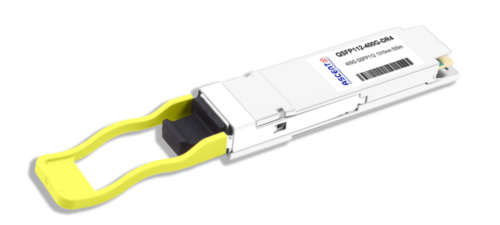
400G QSFP112 DR4 1310 nm 500 m
400G QSFP112 DR4 1310 nm Transceiver 500m
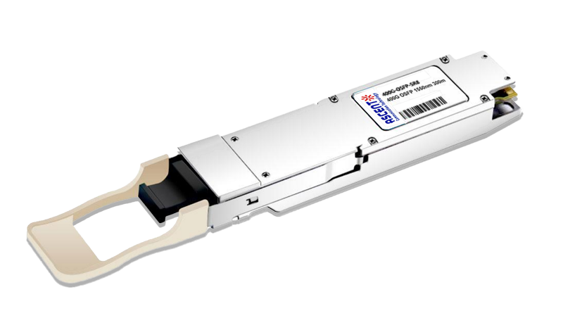
400G OSFP SR4 FLT 50m Transceiver
400 Gbps Multi-Mode 50m OSFP Transceiver
400G OSFP SR8 100m Transceiver
400 Gbps PSM8 Multi-Mode 100m OSFP Transceiver
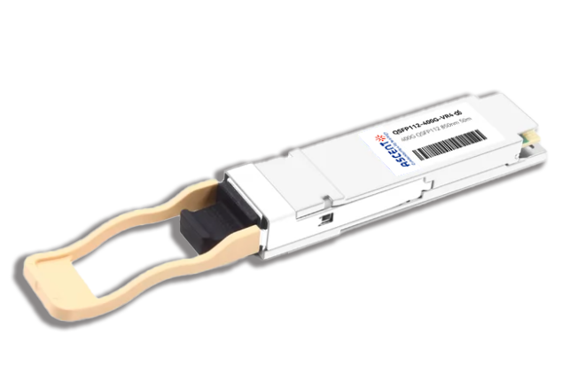
400G QSFP112 VR4 Transceiver
400G QSFP112 VR4
White Paper
Press Releases
Briefings 1
Briefings 2
Videos, etc.
QRG
Manual1
Manual2
Get in touch with our experts
Feedback