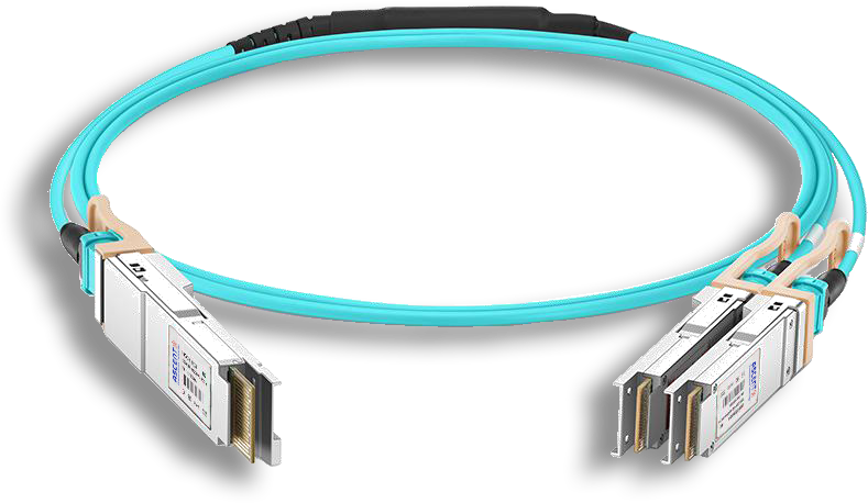
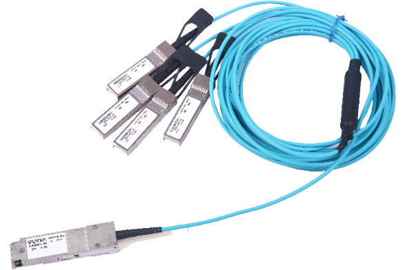
- FIBER OPTIC TRANSCEIVERS >Optical Cables and Accessories >400G OSFP to 2x200G QSFP56 AOC Breakout Cable
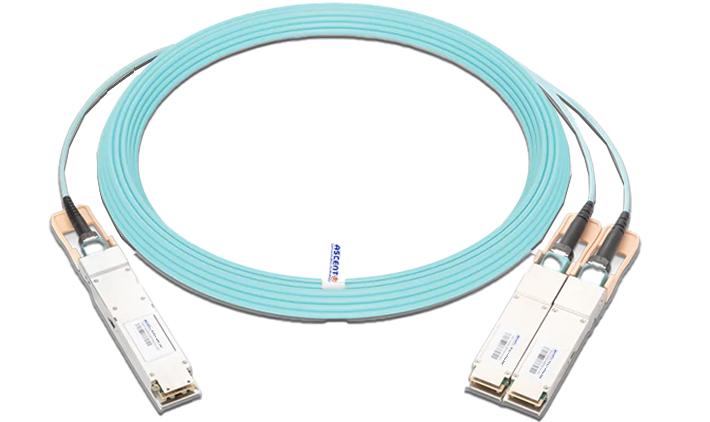
400G OSFP to 2x200G QSFP56 AOC Breakout Cable
Ascentãs 400G OSFP product is an OSFP to 2x QSFP56, 400Gb/s to 2 x 200Gb/s Active Optical Breakout Cable (AOC) designed for connecting Mellanox NDR switch with OSFP cage to legacy 2 Mellanox HDR switch/HCA QSFP56 cages. The cable is compliant with SFF-8665 for the QSFP56 pluggable solution. It provides connectivity between system units with a OSFP 400Gb/s connector on one side and two separate QSFP56 200Gb/s connectors on the other side, such as a switch and two servers. The cable connects data signals from each of the 8 MMF (Multi Mode Fiber) pairs on the single OSFP end to the four pairs of each of the QSFP56 multiport ends. It supports 53.125Gb/s per channel. Ascentãs active fiber cable solutions provide power-efficient connectivity for data center interconnects. It enables higher port bandwidth, density and configurability at a low cost, and reduced power requirement in the data centers. four-channel full-duplex active optical cable. The OSFP cable has low power dissipation and 8x50g PAM VCSEL/PIN photo detector. Its operating case temperature is 0ô¯C~70ô¯C.
ôñ 400Gb/s to 2x200Gb/s data rate
ôñ Programmable Rx output amplitude and pre-emphasis
ôñ OSFP head end is CMIS 4.0 compliant
ôñ QSFP56 ends are SFF-8665 compliant
ôñ 4.5W Max power consumption for QSFP56 ends
ôñ 14W Max power consumption for the OSFP head end
ôñ Single 3.3V power supply
ôñ Hot pluggable
ôñ RoHS compliant
ôñ SFF-8636 compliant I2C management interface
Absolute Maximum Ratings
Parameter | Symbol | Min. | Max. | Unit |
Operating Case Temperature | Top | 0 | +70 | ô¯C |
Storage Temperature Range | Ts | -40 | +85 | ô¯C |
Relative Humidity | RH | 0 | 85 | % |
Power Supply Voltage | Vcc | -0.5 | +3.6 | V |
Recommended Operating Conditions
Parameter | Symbol | Min. | Typ. | Max. | Unit |
Operating Case Temperature Range | Tca | 0 | / | 70 | ô¯C |
Power Supply Voltage | Vcc | 3.135 | 3.3 | 3.465 | V |
Optical Characteristics
This section shows the range of values for normal operation. The host board power supply filtering should be designed as recommended in the SFF Committee Spec.
Parameter | Min. | Typ. | Max. | Unit |
Supply Voltage (Vcc) | 3.135 | 3.3 | 3.465 | V |
Power Consumption 400Gb/s End | - | 4.35 | 4.5 | W |
Power Consumption 400Gb/s End | - | 13 | 14 | W |
Supply Noise Tolerance(10Hz to 10MHz) | 66 | - | - | mVpp |
Operating Case Temperature | 0 | - | 70 | ô¯C |
Operating Relative Humidity | 5 | - | 85 | % |
Electrical Characteristics
Parameter (per lane) | Min. | Typ. | Max. | Unit |
Signaling Rate | -100 ppm | 53.125 | +100 ppm | Gbps |
Differential Data Input Swing at TP1a | TBD | 900 | mVpp | |
Differential Data Output Swing at TP4 | - | - | 900 | mVpp |
Near-End ESMW | 0.265 | - | - | UI |
Near-End Output Eye Height | 70 | - | - | mVpp |
Output Transition Time, 20% to 80% | 9.5 | - | - | ps |
Note:
1. Multiple clock domains are supported only on line-side Rx. Host side Rx supports a single clock domain only.
2. QSFP Tx CDR lock can only occur if Tx lane 4 is transmitting data.
Mechanical Characteristics
Parameter (per lane) | Min. | Unit | |
Diameter | 3 +/-0.2 | mm | |
Differential Data Input Swing at TP1a | TBD | mVpp | |
Length Tolerance | length < 5 m | +300 / -0 | mm |
Near-End ESMW | 5 m ãÊ length < 50 m | +500 / -0 | mm |
Near-End Output Eye Height | 50 m ãÊ length | +1000 / -0 | mm |
Cable Color | Aqua | - | |

Cable Breakout point
Total Length(m) | Breakout*2*200G(m) |
1 | 0.5 |
2 | 0.5 |
3 | 1 |
5 | 2 |
7 | 3 |
10 | 3 |
X (X>10) | 3 |

OSFP 800G ACC Cable
800G Twin-port 2x400G OSFP Active Copper Cable
OSFP 800G DAC Cable
800G Twin-port 2x400G OSFP Passive DAC Cable
800G OSFP to 4x200G Breakout ACC
800G 4x200G OSFP Breakout Active Copper Cable
800G OSFP 4xQSFP112 DAC Cable
800G OSFP to 4xQSFP112 Cable Assembly
400G OSFP to 400G QSFP-DD DAC
400G OSFP to 400G QSFP-DD Passive DAC Twinax Cable

400G OSFP to 4x100G QSFP56 DAC
400G OSFP to 4x100G QSFP56 Passive DAC Breakout Cable

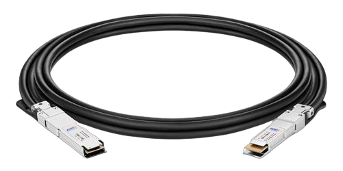
400G QSFP DD DAC Cable
400G QSFP-DD Passive Direct Attach Copper Cable

400G QSFP DD to 4X100G QSFP56 AOC
400G QSFP-DD to 4x100G QSFP56 Active Optical Cable

400G QSFP DD to 4X100G QSFP28 AOC
400G QSFP-DD to 4x100G QSFP28 Active Optical Cable

400G QSFP DD AOC Cable
400G QSFP-DD Active Optical Cable
400G QSFP DD AOC Breakout Cable
400G QSFP-DD to 2x 200G QSFP56 Active Optical Breakout Cable

200G QSFP56 InfiniBand HDR AOC
200G QSFP56 to QSFP56 Active Optical Cable

200G QSFP56 PSM4 DAC
200G QSFP56 PSM4 Direct Attach Passive Copper Cables
QSFP28 100G AOC Cable
100 Gb/s QSFP28 Active Optical Cable
QSFP28 100G DAC Cable
100G QSFP28 Passive DAC Twinax Cable
QSFP AQ AOC 4G 10
40G QSFP+ to 4x10G SFP+ Transceiver

QSFP+ 40G DAC Cable
40G QSFP+ to QSFP+ Passive Copper Cable (PCC)
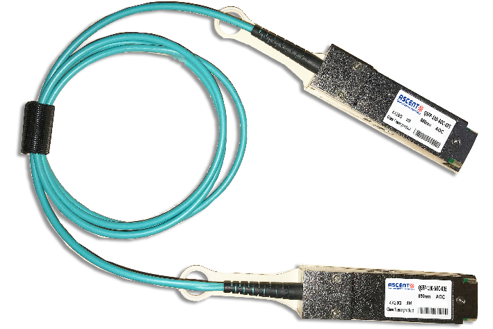
QSFP+ 40G AOC Cable
40G QSFP+ Active Optical Cable
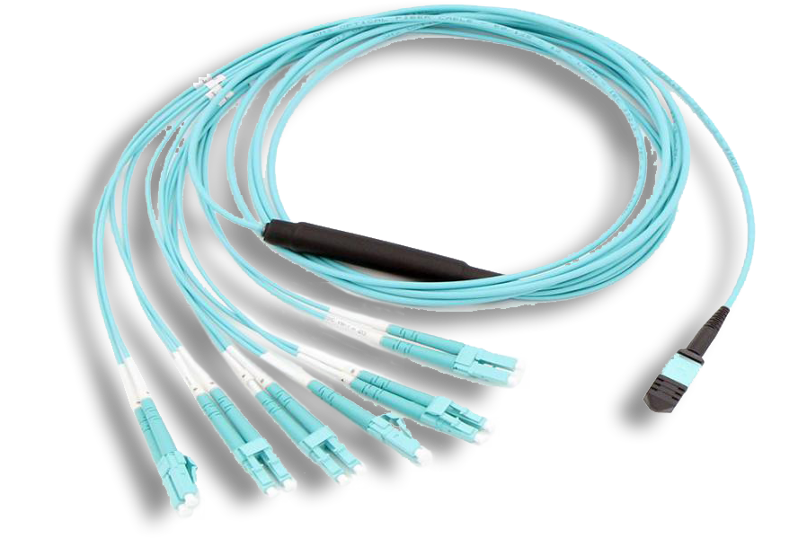
MTP/MPO Harness Assemblies
12/24 MTP/MPO LC Harness Cable Assembly
25G SFP28 AOC Cable
25 Gb/s SFP28 Active Optical Cable DDM
SFPP AT AOC Cable
10G SFP+ Active Optical Cable
100G to 25G Adapter
100G QSFP28 to 25G SFP28 Adapter
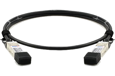
10G SFP+ Passive Copper Twinax Cable
SFPP-AT-DAC-2M 10G SFP+ Passive Direct Attach Copper Twinax Cable (PCC)
White Paper
Press Releases
Briefings 1
Briefings 2
Videos, etc.
QRG
Manual1
Manual2
Get in touch with our experts
Feedback