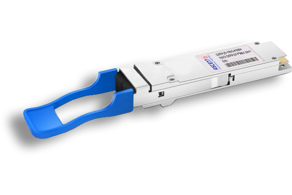
- FIBER OPTIC TRANSCEIVERS >200G & 100G Transceivers >100G QSFP28 SR4 850 nm 100 m
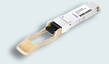
100G QSFP28 SR4 850 nm 100 m
Ascentãs QSFP28-100G-SR01 is a 100Gb/s transceiver module designed for optical communication applications compliant to IEEE 802.3bm standards. The optical transmitter portion of the transceiver incorporates a 4-channel VCSEL (Vertical Cavity Surface Emitting Laser) array, a 4-channel input buffer and laser driver, diagnostic monitors, control and bias blocks. For module control, the control interface incorporates a Two Wire Serial interface of clock and data signals. Diagnostic monitors for VCSEL bias, module temperature, transmitted optical power, received optical power and supply voltage are implemented and results are available through the TWS interface. The optical receiver portion of the transceiver incorporates a 4-channel PIN photodiode array, a 4ãchannel TIA array, a 4-channel output buffer, diagnostic monitors, and control and bias blocks. Diagnostic monitors for optical input power are implemented and results are available through the TWS interface. The product is designed with form factor, optical/electrical connection and digital diagnostic interface according to the QSFP+ Multi-Source Agreement (MSA). It has been designed to meet the harshest external operating conditions including temperature, humidity and EMI interference.
ôñ Hot pluggable QSFP28 MSA form factor
ôñ Compliant to Ethernet 100GBASE-SR4
ôñ Supports 103.1 Gb/s aggregate bit rate
ôñ Up to 100 m reach with OM4 multimode fiber
ôñ Up to 70 m reach with OM3 multimode fiber
ôñ Single +3.3V power supply
ôñ Operating case temperature: 0 ô¯C to 70 ô¯C
ôñ <2.0 W power dissipation
ôñ High reliability 850 nm VCSEL technology
ôñ Standard 12 lane with MPO male connector
ôñ Compliant with SFF-8636
ôñ RoHS and FCC compliant
Absolute Maximum Ratings
Parameter | Symbol | Min. | Typ. | Max. | Unit | Note |
Storage Temperature | TS | ã40 | 85 | ô¯C | ||
Relative Humidity | RH | 5 | 95 | % | ||
Power Supply Voltage | Vcc | ã0.3 | 4.0 | V | ||
Signal Input Voltage | Vccã0.3 | Vcc+0.3 | V |
Recommended Operating Conditions
Parameter | Symbol | Min. | Typ. | Max. | Unit | Note |
Case Operating Temperature | Tcase | 0 | - | 70 | ô¯C | Without air flow |
Power Supply Voltage | Vcc | 3.14 | 3.3 | 3.46 | V | |
Power Supply Current | Icc | - | 600 | mA | ||
Data Rate | BR | 25.78125 | Gbps | Each channel | ||
Transmission Distance | TD | - | 100 | m | OM4 | |
TD | - | 70 | m | OM3 |
Note:
100G Ethernet &100GBASE-SR4 and ITU-T OTU4 has different register setting, not auto-negotiation
Optical Characteristics
Parameter | Symbol | Min. | Typ. | Max. | Unit | Note |
| Transmitter | ||||||
Case Operating Temperature | ö£0 | 840 | 860 | nm | ||
Average Launch Power each lane | -8.4 | 2.4 | dBm | |||
Spectral Width (RMS) | ü | 0.6 | nm | |||
Optical Extinction Ratio | ER | 3 | dB | |||
Optical Return Loss Tolerance | ORL | 12 | dB | |||
Output Eye Mask | Compliant with IEEE 802.3bm-2015 | 1 | ||||
Receiver | ||||||
Receiver Wavelength | ö£in | 840 | 860 | nm | ||
Rx Sensitivity per lane | RSENS | -10.3 | dBm | 2 | ||
LOS De-Assert | LOSD | -30 | dBm | |||
LOS Assert | LOSA | -12 | dBm | |||
Input Saturation Power (Overload) | Psat | 2.4 | dBm | |||
Receiver Reflectance | Rr | -12 | dB | |||
Notes:
1. Hit ratio 1.5*10-5 hits per sample
2. Measured with a PRBS 231-1 test pattern, @ 25.78 Gb/s, BER<10-12.
Electrical Characteristics
Parameter | Symbol | Min. | Typ. | Max. | Unit | Note |
Supply Voltage | Vcc | 3.14 | 3.3 | 3.46 | V | |
Supply Current | Icc | 600 | mA | |||
Transmitter | ||||||
Input Differential Impedance | Rin | 100 | öˋ | 1 | ||
Differential Data Input Swing | Vin, pp | 180 | 1000 | mV | ||
Single Ended Input Voltage Tolerance | VinT | -0.3 | 4.0 | V | ||
Receiver | ||||||
Differential Data Output Swing | Vout, pp | 300 | 850 | mV | 2 | |
Single-Ended Output Voltage | -0.3 | 4.0 | V |
Notes:
1. Connected directly to TX data input pins. AC coupled there after.
2. Into 100 öˋ differential termination.


200G QSFP DD LR4 10km
200 Gb/s QSFP DD LR4 10 km Transceiver
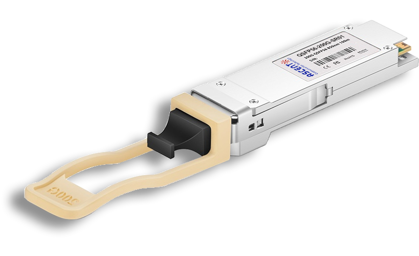
200G QSFP56 SR4 850 nm 100 m
QSFP56-200G-SR01 200 Gb/s QSFP56 SR4 850 nm 100 m Transceiver

100G QSFP28 LX4 2km
100 Gb/s 2km QSFP28 LX4 Transceiver

100G QSFP28OA LR4 10km
100 Gb/s 10 km QSFP28 LR4 Transceiver

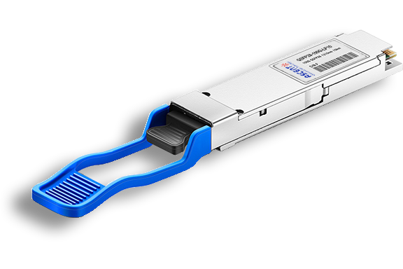
100G QSFP28 ZR4 1310 nm 80 km
QSFP28-100G-LP80 QSFP28 100 Gbps ZR4 Transceiver

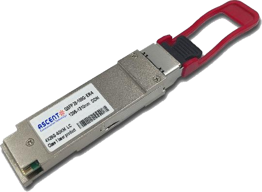
100G QSFP28 ER4L 1310 nm 40 km
QSFP28-100G-LP40 100 Gb/s 40 km QSFP28 ER4 Lite Transceiver
100G QSFP28 ER4 1310 nm 40 km
100 Gb/s 40 km QSFP28 ER4 Transceiver
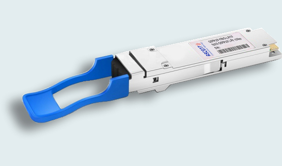
100G QSFP28 LR4 1310 nm 10 km
QSFP28-100G-LP10 100 Gb/s 10km QSFP28 LR4 Transceiver
100G QSFP28 LR Single ö£ 10 km
100G QSFP28 LR1 10 km Single Channel

100G QSFP28 DR Single ö£ 500 m
QSFP28 100G DR Single Lambda Transceiver
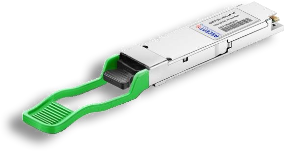
100G QSFP28 CWDM4 1310 nm 2 km
QSFP28-100G-LP02 QSFP28 100 Gbps CWDM4 Transceiver
100G QSFP28 PSM4 1310 nm 2 km
QSFP28-100G-PSM4 100 Gb/s 1310 nm 2 km Transceiver
100G QSFP28 FR Single ö£ 1310 nm 2 km
100G QSFP28 FR 2km Transceiver

100G QSFP28 SR01 BIDI MMF 850nm 100m
QSFP28 BIDI 100 Gb/s SR Transceiver 100m

100G QSFP28 BIDI 80km
QSFP28 BIDI 100 Gb/s ZR4 Transceiver 80km

100G QSFP28 BIDI 40km
QSFP28 BIDI 100 Gb/s ER Transceiver 40km

100G QSFP28 EZR4 100km
QSFP28 100Gb/s EZR4 Transceiver 100km

100G SFP56 ER1 30km
SFP56-DD 100G-ER1 Optical Transceiver 30km

100G SFP56 LR1 10km
SFP56-DD 100G-LR1 Optical Transceiver 10km
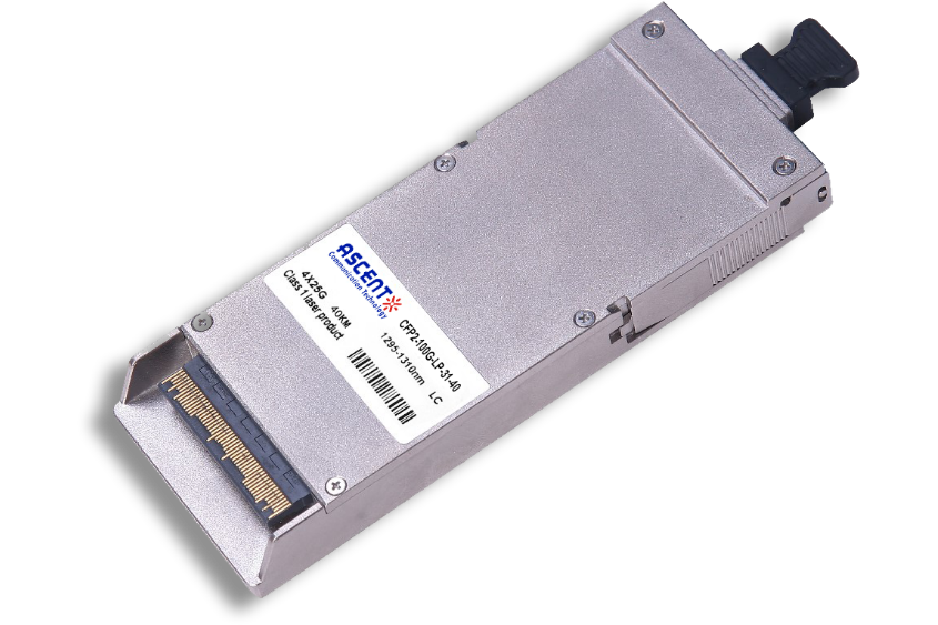
100G CFP2 ER4 40 km
CFP2-LP-31-40 100 Gb/s CFP2 ER4 40 km Transceiver
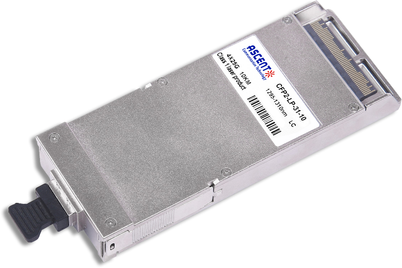
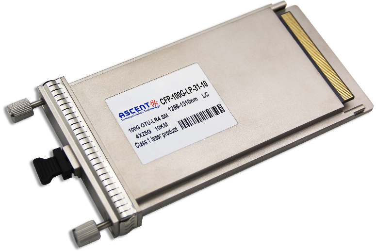
100G CFP2 LR4 10 km
CFP2-LP-31-10 100 Gb/s CFP2 LR4 10 km Transceiver
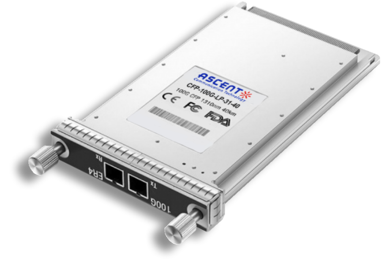
100G CFP ER4 40 km
CFP-LP-31-40 100 Gb/s CFP ER4 40 km Transceiver
100G CFP LR4 10 km
CFP-LP-31-10 100 Gb/s CFP LR4 10 km Transceiver
White Paper
Press Releases
Briefings 1
Briefings 2
Videos, etc.
Manual1
Manual2
Get in touch with our experts
Feedback