- FIBER OPTIC TRANSCEIVERS >800G & 400G Transceivers >400G QSFP112 VR4 Transceiver
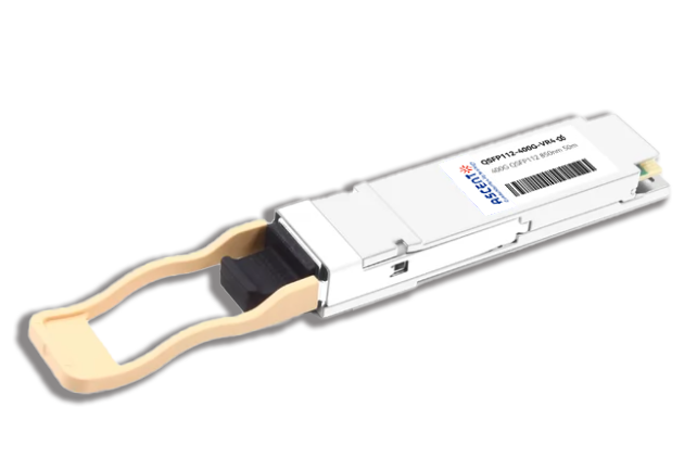
400G QSFP112 VR4 Transceiver
The 400G QSFP112 VR4 transceiver is a high-performance, short-reach optical module designed for next-generation 400G Ethernet and InfiniBand applications in hyperscale data center environments. Utilizing four parallel optical lanes operating at 106.25Gb/s PAM4, the module delivers an aggregate bandwidth of up to 425Gb/s over multimode fiber, supporting transmission distances of up to 50 meters on OM4 MMF. Its compact QSFP112 Type 1 form factor enables high-density deployment in modern switch, router, and AI cluster architectures. The module incorporates advanced 850nm VCSEL transmitters and PIN receivers with a high-speed 400GAUI-4 electrical interface, providing excellent signal integrity and low latency performance for demanding data center interconnect applications. The optical interface utilizes a standard MPO-12 connector, enabling efficient parallel fiber connectivity for high-speed networking infrastructure. Designed for optimized thermal and EMI performance, the transceiver supports reliable operation in dense networking systems while maintaining low power consumption. Fully compliant with 400G QSFP112 MSA and CMIS 4.0 management interface standards, it supports comprehensive digital diagnostics and control functions for real-time system monitoring and management. Operating from a single +3.3V power supply over a commercial temperature range of 0ô¯C to +70ô¯C, the module is RoHS compliant and designed to meet industry Class 1 laser safety standards, making it an ideal solution for high-speed cloud, AI, and enterprise data center networks.
ôñ Support 100GBASE per lane in multimode fiber
ôñ Hot-pluggable QSFP112 Type 1 form factor
ôñ Data rate up to 425Gbps (4x 106.25 Gbps)
ôñ Reach up to 50m on MMF (OM4)
ôñ 850nm VCSEL laser and PIN receiver
ôñ High speed I/O electrical interface (400GAUI-4)
ôñ Single MPO-12 receptacle
ôñ Operating case temperature: 0 to +70ô¯C
ôñ Compliant to RoHS 6/6
ôñ Compliant to 400G QSFP112 MSA and CMIS4.0
Parameter | Symbol | Min. | Max. | Unit | Note |
Operating Case Temperature | TOP | 0 | 70 | ô¯C | 1,2 |
Power Supply Voltage | Vcc | -0.5 | 3.6 | V | |
Storage Temperature Range | TST | -40 | 85 | ô¯C | 1,2 |
Operating Relative Humidity | RH | 5 | 85 | % | 1,2,3 |
Notes:
1. Absolute Maximum Ratings are those beyond which damage to the device may occur.
2. Between the Recommended Operating conditions and Absolute Maximum ratings, prolonged operation is not intended, and permanent device degradation may occur.
3. Non-condensing.
Optical Characteristics
Parameter | Symbol | Min. | Typ. | Max. | Unit | Note |
Transmitter | ||||||
Signaling Rate, each Lane | - | 53.125 ôÝ 100 ppm | GBd | |||
Modulation Format | - | PAM4 | - | |||
Center Wavelength | ö£C | 842 | - | 948 | nm | |
RMS Spectral Width | - | - | - | 0.65 | nm | 1 |
Average Launch Power, each Lane | AOPL | -4.6 | - | 4 | dBm | |
Outer Optical Modulation Amplitude (OMAouter), each Lane | TOMA | - | - | 3.5 | dBm | |
Outer Optical Modulation Amplitude (OMAouter), each Lane for Max(TECQ, TDECQ)ãÊ1.8 dB for 1.8ÿ¥Max(TECQ, TDECQ)ãÊ4.4 dB | TOMA | -2.6 -4.4 | - | - | dBm | |
Transmitter and Dispersion Eye Closure for PAM4 (TDECQ), each Lane | TDECQ | - | - | 4.4 | dB | |
Transmitter Eye Closure for PAM4 (TECQ), each Lane | TECQ | - | - | 4.4 | dB | |
Overshoot/Undershoot | - | - | - | 29 | % | |
Transmitter Power Excursion, each Lane | - | - | - | 2.3 | dBm | |
Extinction Ratio | ER | 2.5 | - | - | dB | |
Transmitter Transition Time, each Lane | - | - | - | 17 | ps | |
Average Launch Power of OFF Transmitter, each Lane | TOFF | - | - | -30 | dBm | |
RIN12OMA | RIN | - | - | -132 | dB/Hz | |
Optical Return Loss Tolerance | ORL | - | - | 14 | dB | |
Encircled Flux | - | ãË86% at 19 nm ãÊ30% at 4.5um | - | 2 | ||
Receiver | ||||||
Signaling Rate, each Lane | - | 53.125 ôÝ 100 ppm | GBd | |||
Modulation Format | - | PAM4 | - | |||
Center Wavelength | ö£C | 842 | - | 948 | nm | |
Damage Threshold | AOPD | 5 | - | dBm | 3 | |
Average Receive Power, each Lane | AOPR | -6.3 | - | 4 | dBm | |
Receive Power, each Lane (OMAouter) | OMAR | - | - | 3.5 | dBm | |
Receiver Reflectance | RR | - | - | -15 | dB | |
Receiver Sensitivity (OMAouter), each Lane for TECQãÊ1.8 dB for 1.8ÿ¥TECQãÊ4.4 dB | SOMA | - | - | - -4.4 -6.2 | dBm | |
Stressed Receiver Sensitivity (OMAouter), each Lane | SRS | - | - | -1.8 | dBm | 4 |
Conditions of Stressed Receiver Sensitivity Test | 5 | |||||
Stressed Eye Closure for PAM4 (SECQ) | - | - | 4.4 | - | dB | |
SECQ ã 10log10(Ceq), Lane Under Test | - | - | - | 4.4 | dB | |
OMAouter of Each Aggressor Lane | - | - | 3.5 | - | dBm | |
Note:
1. RMS spectral width is the standard deviation of the spectrum.
2. If measured into type A1a.2 or type A1a.3, or A1a.4, 50 ö¥m fiber, in accordance with IEC 61280-1-4.
3. The receiver shall be able to tolerate, without damage, continuous exposure to an optical input signal having this average power level on one lane. The receiver does not have to operate correctly at this input power.
4. Measured with conformance test signal at TP3 (see 167.8.14) for the BER specified in 167.1.1.
5. These test conditions are for measuring stressed receiver sensitivity. They are not characteristics of the receiver.
Electrical Characteristics
Parameter | Symbol | Min. | Typ. | Max. | Unit | Note |
Transmitter | ||||||
Signaling Rate, each Lane | - | 53.125 ôÝ 50 ppm | GBd | |||
Differential Pk-Pk Input Voltage Tolerance | - | 900 | - | - | mV | |
Differential to Common-Mode Return Loss | RLcd | 802.3ck 120G-2 | dB | |||
Effective Return Loss | ERL | 8.5 | - | - | dB | |
Differential Termination Mismatch | - | - | - | 10 | % | |
Module Stressed Input Tolerance | See 120G.3.4.3 | - | ||||
Single-Ended Voltage Tolerance Range | - | -0.4 | - | 3.3 | V | |
DC Common-Mode Voltage | - | -350 | - | 2850 | mV | 1 |
Receiver | ||||||
Signaling Rate, each Lane | - | 53.125 ôÝ 50 ppm | GBd | |||
AC Common-Mode Output Voltage | - | - | - | 17.5 | mV | |
Differential Peak-to-Peak Output Voltage Short Mode Long Mode | - | - | - | - 600 900 | mV | |
Eye Height | EH | 15 | - | - | mV | |
Vertical Eye Closure | VEC | - | - | 12 | dB | |
Common-Mode to Differential Return Loss | RLDc | 802.3ck 120G-2 | dB | |||
Effective Return Loss, ERL | ERL | 8.5 | - | - | dB | |
Differential Termination Mismatch | - | - | - | 10 | % | |
Transition Time | - | 8.5 | - | - | ps | |
DC Common-Mode Voltage1 | Tr/Tf | -350 | - | 2850 | mV | 2 |
Power Supply | 3 | |||||
Power Supply Voltage | VCC1, VCCTx, VCCRx | 3.13 | 3.30 | 3.47 | V | |
Power Consumption | PW | - | - | 10 | W | |
Power Consumption-LP mode | - | - | - | 1.5 | W | |
Notes:
1. DC common-mode voltage generated by the host. Specification includes effects of ground offset voltage.
2. The signaling rate range is derived from the PMD receiver input. DC common-mode voltage is generated by the host. Specification includes effects of ground offset voltage.
3. The specified characteristics are met within the recommended range of operation. Unless otherwise noted typical data are quoted at nominal voltage and +25ô¯C ambient temperature.

Notes:
1. All dimensions shown are in millimeters.
2. Tolerances are in accordance with QSFP112 MSA.
800G OSFP DAC Cable
800G IB NDR OSFP to 4xOSFP RHS Hairtail+ Direct Attach Copper Cable
800G OSFP ACC Cable
800G OSFP Breakout to 4x200G OSFP Active Copper Cable

800G OSFP DR8 1310 nm 500 m
800 Gb/s DR8 OSFP 500m Optical Transceiver

800G OSFP SR8 850 nm 100 m
OSFP-800G-SR8D-01 800 Gb/s OSFP SR8 850 nm 100 m Transceiver
400G QSFP56-DD 10km
400G QSFP-DD 4X100G LR1 Optical Transceiver

400G QSFP-DD ZR+
QSFP-DD-ZR-80 400 Gb/s QSFP-DD 80 km Transceiver
400G QSFP-DD ER8 40 km
QSFP-DD-ER8-40 400 Gb/s QSFP-DD 40 km Transceiver
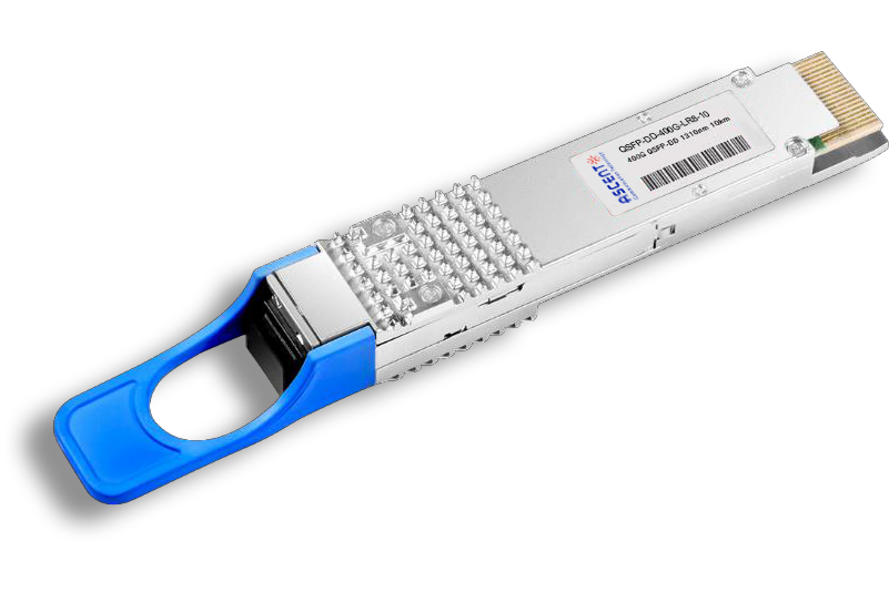
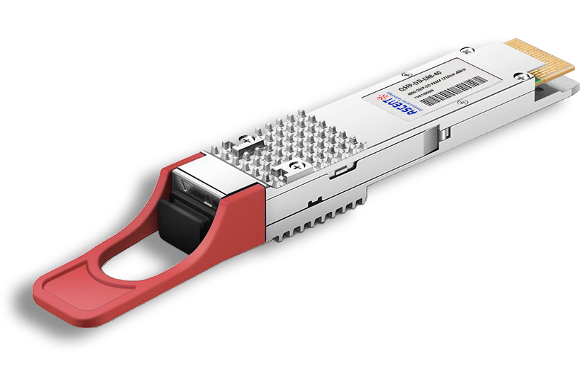
400G QSFP-DD LR8 1310 nm 10 km
QSFP-DD-LR8-10 400 Gb/s QSFP-DD LR8 10 km Transceiver

400G QSFP-DD LR4 CWDM 10 km
QSFP-DD-LR4-10 400 Gb/s QSFP-DD LR4 CWDM 10 km Transceiver
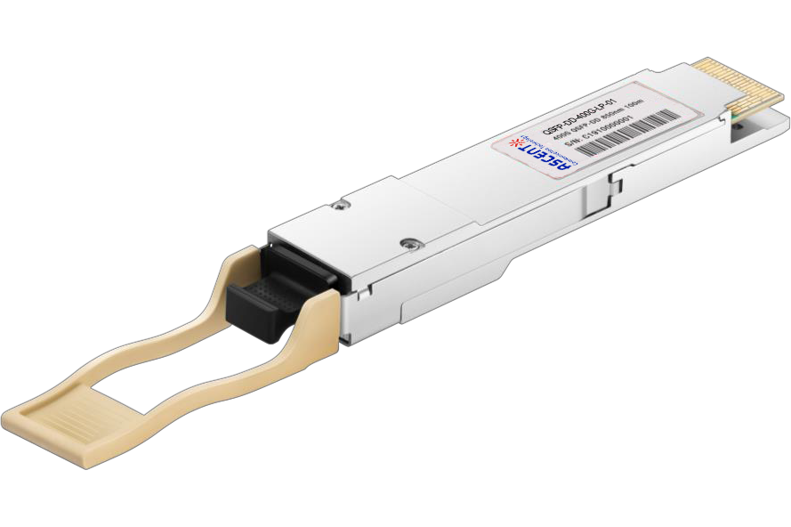
400G QSFP-DD SR8 850 nm 100 m
QSFP-DD-LP-01 400 Gb/s QSFP-DD SR8 100 m Transceiver
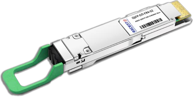
400G QSFP-DD FR4 2km
400 Gb/s QSFP-DD FR4 2 km DDM Transceiver

400G QSFP-DD DR4 500m
400 Gb/s QSFP-DD DR4 500m Transceiver

400G QSFP-DD DCO ZR
400G QSFP-DD DCO ZR Coherent Optical Transceiver

4X100G QSFP-DD LR4 10km
QDD 4x100G 1310nm LR 10 km Transceiver
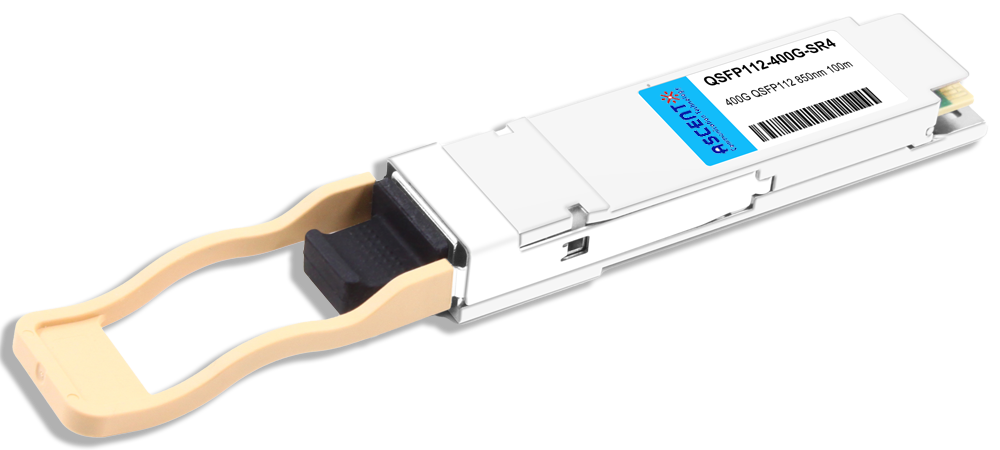
400G QSFP112 SR4 850 nm 100 m
QSFP112-400G-SR4-01 400 Gb/s QSFP112 SR4 850 nm 100 m Transceiver
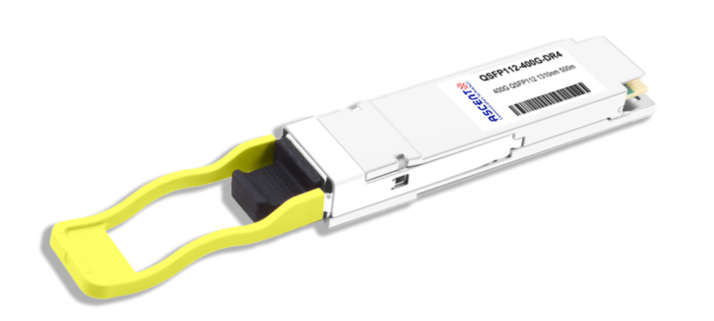
400G QSFP112 DR4 1310 nm 500 m
400G QSFP112 DR4 1310 nm Transceiver 500m
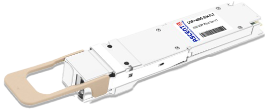
400G OSFP SR4 FLT 50m Transceiver
400 Gbps Multi-Mode 50m OSFP Transceiver
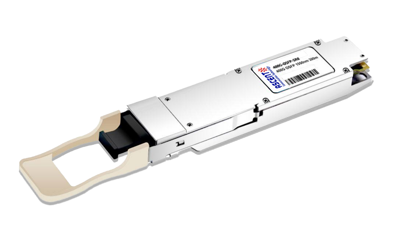
400G OSFP SR8 100m Transceiver
400 Gbps PSM8 Multi-Mode 100m OSFP Transceiver
White Paper
Press Releases
Briefings 1
Briefings 2
Videos, etc.
QRG
Manual1
Manual2
Get in touch with our experts
Feedback