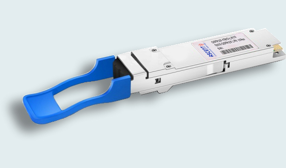
- FIBER OPTIC TRANSCEIVERS >200G & 100G Transceivers >100G QSFP28 FR 1310 nm 2 km

100G QSFP28 FR 1310 nm 2 km
Ascentãs 100G FR1 2km SFP-DD duplex LC transceiver, is a fully integrated, 53.125GBaud PAM4 single optical channel transceiver. The optical channel uses a 4-level pulse amplitude modulation(PAM4) format by means of a DSP, a 1310 nm wavelength EA-DFB laser diode, a PIN photo-diode connecting to a PAM4-based 2 channel x 26.5625GBaud 100GAUI-2 electrical interface by means of a 2:1 mux/demux. This single optical channel technology enables a cost-optimized solution for 100GE optical links. The CMIS compliant 2-wire management interface enables control, alarm and monitoring of the SFP-DD module. The 100GBASE-FR Single Lambda SFP-DD module is designed for use in 100GBASE Ethernet throughput up to 2km over single mode fiber (SMF) using a wavelength of 1310nm via duplex LC connectors. This transceiver is compliant with SFPDD MSA and SFP-DD MIS Rev 2.0 standard. It combines 2x26.5625GBd PAM4 electrical lane sin to one 53.125GBd PAM4 optical channel in compliance with IEEE100GBASE-FR. With these features, this easy to install, hot swappable transceiver is suitable to be used in various applications, such as Data Center, 100G Ethernet.
ôñ IEEE 100GBASE-FR Compliant
ôñ 100GAUI-2 Compliant-2x 26.5625Gbaud
ôñ SFP-DD MSA Compliant
ôñ 3.5W Max Power Consumption (3.0W typ)
ôñ Operating case temperature range: 0 to 70ô¯C
ôñ Single Cooled 100Gb/s 1310nm EML
ôñ Single PIN PD+Low-power TIA
ôñ CMIS Management Interface
Absolute Maximum Ratings
Stresses in excess of the absolute maximum ratings can cause permanent damage to the device. These are absolute stress ratings only. Functional operation of the device is not implied at the seorany other conditions in excess of those given in the operational sections of the datasheet. Exposure to absolute maximum ratings will cause permanent damage and/or adversely affect device reliability.
Parameter | Symbol | Min. | Max. | Unit | Notes |
Supply Voltage | Vcc | 0 | 3.6 | V | +3.3 |
Storage Temperature | -40 | 85 | ô¯C | ||
Optical Receiver Input | - | +5.5 | dBm | Average |
Recommended Operating Conditions
Electrical and optical characteristics below are defined under this operating environment, unless otherwise specified.
Parameter | Symbol | Min. | Typ. | Max | Unit | Notes |
Supply Voltage | Vcc | 3.135 | 3.3 | 3.465 | V | |
Supply Voltage Noise Tolerance | PSNR | - | - | 66 | mV | 10Hz to 10MHz |
Power Consumption | - | 3.0 | 3.5 | W | ||
Supply Current | - | - | 1116.4 | mA | Steady state | |
Case Temperature | Tc | 0 | 25 | 70 | ô¯C |
Optical Characteristics
Parameter | Min | Typ. | Max | Unit | Notes |
PAM4 Signaling Rate (Range) | 53.125 + 100 ppm | GBd | |||
Lane Wavelengths (Range) | 1304.5 | 1317.5 | nm | ||
Side-Mode Suppression Ratio (SMSR), (Min) | 30 | dB | |||
Average Launch Power (Max) | 4 | dBm | |||
Average Launch Power (Min) | -3.1 | dBm | 1 | ||
Outer Optical Modulation Amplitude (OMAouter) (Max) | 4.2 | dBm | |||
Outer Optical Modulation Amplitude (OMAouter) (Min) forTDECQ<1.4 dB | -0.1 | dBm | |||
Outer Optical Modulation Amplitude (OMAouter) (Min) for 1.4dB STDECQ<3.4 dB | -1.5+TDECQ | dBm | |||
Transmitter and Dispersion Penalty Eye Closure for PAM4TDECQ),(Max) | 3.4 | dB | |||
Transmitter Eye Closure for PAM4 (TECQ) (Max) | 3.4 | dB | |||
TDECQ-TECQ (Max) | 2.5 | dB | |||
Over/Under-Shoot (Max) | 22 | % | |||
Transmitter Power Excursion (max) | 2 | dBm | |||
| Average Launch Power of OFF Transmitter | -15 | dBm | |||
Extinction Ratio (Min) | 3.5 | dB | |||
Optical Return Loss Tolerance (Max) | 17.1 | dB | |||
Transmitter Reflectance (Max) | -26 | dB | 2 | ||
Transmitter Tansition Time (Max) | 17 | ps | |||
RIN15.5 OMA (Max) | -136 | dB/Hz | |||
Receiver | |||||
PAM4 Signaling Rate (Range) | 53.125+ 100 ppm | GBd | |||
Lane Wavelengths (Range) | 1304.5 | 1317.5 | Nm | ||
Damage Threshold (min) | 5 | dBm | 3 | ||
Average Receive Power (max) | 4 | dBm | |||
Average Receive Power (min) | -7.1 | dBm | 4 | ||
Receive Power (OMAouter) (Max) | 4.2 | dBm | |||
Receiver Reflectance (Max) | -26 | dB | |||
Receiver Sensitivity (OMAouter) (Max) | -4.5, TE -5.9, (See Below Figure Receiver Sensitvity) | dBm | 5 | ||
Stressed Receiver Sensitivity (OMAouter) (max) | -2.5 | 6 | |||
Conditions of Stressed Receiver Sensitivity Test | 7 | ||||
Stressed Eve Closure for PA4 (SECQ) | 3.4 | dB | |||
SECQ-10*log10(Ceg)(max) | - | dB | 8 | ||
1. Average launch power (min) is informative and not the principal indicator of signal strength. A transmitter with launch power below this value cannot be compliant: however a value above this does not ensure compliance.
2. Transmitter reflectance is defined looking into the transmitter.
3. The receiver shall be able to tolerate, without damage, continuous exposure to an optical signal having this average power level.
4. Average receive power, each lane (min) is informative and not the principal indicator of signal strength. A received power below this value cannot be compliant: however a value above this does not ensure compliance.
5. Receiver sensitivity (OMAouter), (max) is informative and is defined for a transmitter with a value of SECQ up to 3.4dB.
6. Measured with conformance test signal at TP3 (see lEEE Std 802.3cd clause 140.7.10) for the BER specified in IEEE Std 802.3cd clause 140.1.1.
7. These test conditions are for measuring stressed receiver sensitivity. They are not characteristics of the receiver.
8. Ceq is a coefficient defined in lEEE Std 802.3-2018 clause 121.8.5.3 which accounts for reference equalizer noise enhancement.
OMA Outer
Receiver Sensitivity

RX LOS Alarm Characteristics
Parameter | Symbol | Min. | Max | Unit | Notes |
Receiver Loss of Signanl Indicator Assert level | -15 | -7.5 | dBm | Average power | |
Receiver Loss of Signanl Indicator Deassert level | RX_LOS | - | -7 | dBm | Average power |
Hysteresis | 0.5 | - | dB |
Electrical Characteristics
Parameter | Min. | Typ. | Max | Unit | Notes |
Module Output (per Lane, at TP4) | 1 | ||||
Signaling Rate per Lane (Range) | -100ppm | 26.5625 | +100ppm | GBd | |
AC Common-Mode Output Voltage (RMS) | - | - | 17.5 | mV | |
Differential Peak-to-Peak Output Voltage | - | - | 900 | mV | |
Near-end ESMW (Eye Symmetry Maskwidth) | 0.265 | - | - | UI | |
Near-end Eye Height, Differential | 70 | mV | |||
Far-end ESMW (Eye Symmetry Maskwidth) | 0.2 | - | - | UI | |
Far-end Eye Height, Differential | 30 | - | - | mV | |
Far-end Pre-cursor ISI Ratio | -4.5 | - | 2.5 | % | |
Differential Output Return Loss | Equation (83E-2) | - | - | dB | 2 |
Common to Differential Mode Conversion Return Loss | Equation (83E-3) | - | - | dB | 2 |
Differential Termination Mismatch | - | - | 10 | % | |
Transition Time (20% to 80%) | 9.5 | - | - | ps | |
DC Common Mode Voltage | -350 | - | 2850 | mV | |
Module Input (per Lane, at TP1) | |||||
Signaling Rate per Lane (Range) | -100ppm | 26.5625 | +100ppm | GBd | |
Differential Pk-Pk Input Voltage Tolerance | 900 | - | - | mV | at TP1a |
Differential Input Return Loss | Equation (83E-5) | - | - | dB | at TP1, Note 2 |
Differential to Common Mode Input Return Loss | Equation (83E-6) | - | - | dB | at TP1. Note 2 |
Differential Termination Mismatch | - | - | 10 | % | at TP1 |
ESMW (Eye Symmetry Mask Width) | 0.22 | - | - | UI | at TP1a |
Eye Width | 0.22 | - | - | UI | at TP1a |
Eye Height | 32 | - | - | mV | at TP1a |
Single-ended Input Voltage Tolerance Range | -0.4 | - | 3.3 | V | at TP1a |
DC Common Mode Voltage | -350 | - | 2850 | mV | at TP1 |
1. Electrical module output is squelched for loss of optical input signal.
2. IEEE 802.3-2018 Section 6.


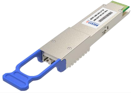
200G QSFP DD LR4 10km
200 Gb/s QSFP DD LR4 10 km Transceiver
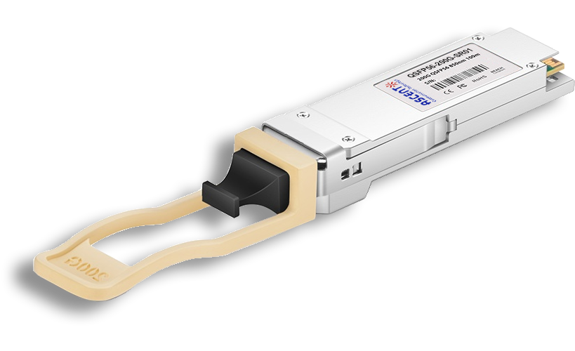
200G QSFP56 SR4 850 nm 100 m
QSFP56-200G-SR01 200 Gb/s QSFP56 SR4 850 nm 100 m Transceiver

100G QSFP28 LX4 2km
100 Gb/s 2km QSFP28 LX4 Transceiver

100G QSFP28OA LR4 10km
100 Gb/s 10 km QSFP28 LR4 Transceiver

100G QSFP28 ZR4 1310 nm 80 km
QSFP28-100G-LP80 QSFP28 100 Gbps ZR4 Transceiver

100G QSFP28 ER4L 1310 nm 40 km
QSFP28-100G-LP40 100 Gb/s 40 km QSFP28 ER4 Lite Transceiver
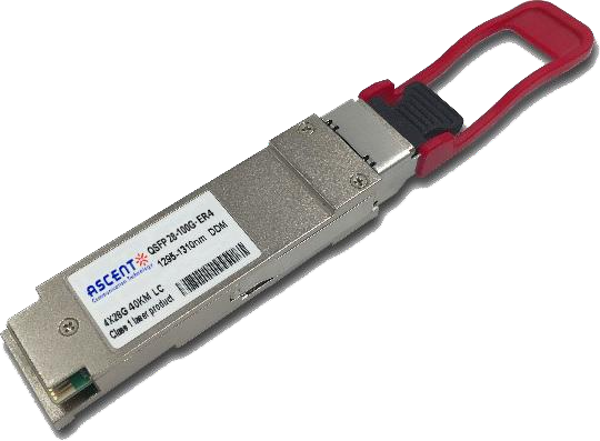
100G QSFP28 ER4 1310 nm 40 km
100 Gb/s 40 km QSFP28 ER4 Transceiver
100G QSFP28 LR4 1310 nm 10 km
QSFP28-100G-LP10 100 Gb/s 10km QSFP28 LR4 Transceiver
100G QSFP28 LR Single ö£ 10 km
100G QSFP28 LR1 10 km Single Channel

100G QSFP28 DR Single ö£ 500 m
QSFP28 100G DR Single Lambda Transceiver
100G QSFP28 CWDM4 1310 nm 2 km
QSFP28-100G-LP02 QSFP28 100 Gbps CWDM4 Transceiver
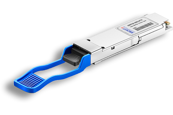
100G QSFP28 PSM4 1310 nm 2 km
QSFP28-100G-PSM4 100 Gb/s 1310 nm 2 km Transceiver
100G QSFP28 SR4 850 nm 100 m
QSFP28-100G-SR01 100 Gb/s SR4 850 nm 100 m Transceiver

100G QSFP28 FR Single ö£ 1310 nm 2 km
100G QSFP28 FR 2km Transceiver

100G QSFP28 SR01 BIDI MMF 850nm 100m
QSFP28 BIDI 100 Gb/s SR Transceiver 100m

100G QSFP28 BIDI 80km
QSFP28 BIDI 100 Gb/s ZR4 Transceiver 80km

100G QSFP28 BIDI 40km
QSFP28 BIDI 100 Gb/s ER Transceiver 40km

100G QSFP28 EZR4 100km
QSFP28 100Gb/s EZR4 Transceiver 100km

100G SFP56 ER1 30km
SFP56-DD 100G-ER1 Optical Transceiver 30km

100G SFP56 LR1 10km
SFP56-DD 100G-LR1 Optical Transceiver 10km
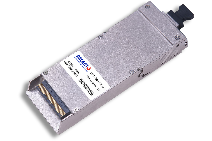
100G CFP2 ER4 40 km
CFP2-LP-31-40 100 Gb/s CFP2 ER4 40 km Transceiver
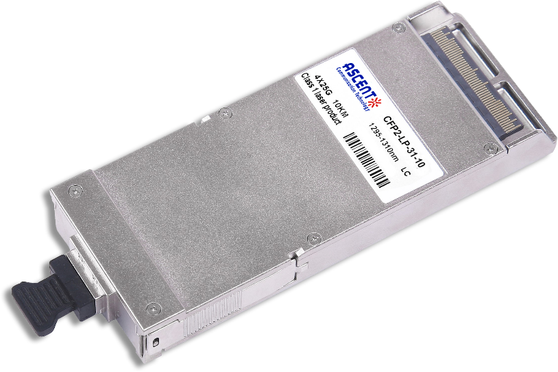
100G CFP2 LR4 10 km
CFP2-LP-31-10 100 Gb/s CFP2 LR4 10 km Transceiver
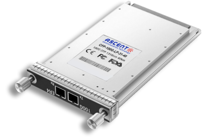
100G CFP ER4 40 km
CFP-LP-31-40 100 Gb/s CFP ER4 40 km Transceiver
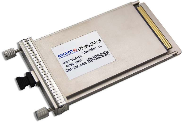
100G CFP LR4 10 km
CFP-LP-31-10 100 Gb/s CFP LR4 10 km Transceiver
White Paper
Press Releases
Briefings 1
Briefings 2
Videos, etc.
QRG
Manual1
Manual2
Get in touch with our experts
Feedback