ASCENT’s XFP-LP-2733-20 and XFP‑LP‑3327‑ 20 Small Form Factor 10 G (XFP) transceivers are compliant with the current XFP Multi-Source Agreement (MSA) Specification. They feature a 1330 nm or 1270 nm DFB transmitter, and a 1270 nm or 1330 nm receiver. They can carry a 10 Gbps data signal up to 20 km over a 9/125 µm SMF wire. Digital diagnostics functions are available via a 2-wire serial interface, as specified in the XFP MSA. The transceiver is RoHS compliant and lead-free per Directive 2002/95/EC3. 10GBASE-LRLW Ethernet per IEEE 802.3ae and 10G Fiber Channel. SONETOC-192, SDH STM I64.1.1200-SMLL-L 10G Fibre Channel.
· Compliant with XFP MSA
· Operating data rate up to 10 Gbps
· 1330 nm DFB transmitter / 1270 nm receiver or 1270 nm DFB transmitter / 1330 nm receiver
· 20 km with 9/125 µm SMF
· Hot-pluggable XFP footprint single LC connector interface
· Power dissipation<2 W
· Class 1 FDA and IEC60825-1 laser safety compliant
· Operating temperature: Standard: 0 °C to +70 °C, Industrial: -40 °C to +85 °C
· 2-wire interface for integrated Digital Diagnostic Monitoring
· Compliant with SFF-8472
Parameter | Symbol | Min. | Max. | Unit |
Storage Temperature | Ts | -40 | +85 | °C |
Maximum Supply Voltage | Vcc | -0.5 | 3.6 | V |
Operating Relative Humidity | 95 | % |
*Exceeding any one of these values may destroy the device.
Parameter Operating Case Temperature | Symbol Tc | Min. 0 | Typ. | Max. +70 | Unit °C | Note Commercial |
-40 | +85 | °C | Industrial | |||
Power Supply Voltage | Vcc | 3.15 | 3.3 | 3.45 | V | |
Power Supply Current | Icc | 580 | mA | |||
Data Rate | 10.3125 | Gbps |
Parameter | Symbol | Min. | Typ. | Max. | Unit | Note |
9µm Core Diameter SMF | 20 | km | ||||
Data Rate Transmitter Centre Wavelength |
λC |
1320 | 9.953/10.3125
1330 |
1340 | Gbps
nm | |
Spectral Width (-20 dB) | ∆λ | 1 | nm | |||
Average Output Power | Pout, AVG | -5 | 0 | dBm | 1 | |
Optical Extinction Ratio | ER | 3.5 | dB | |||
Side Mode Suppression Ratio | SMSR | 30 | dB | |||
Transmitter and Dispersion Penalty | TDP | 2 | dB | |||
Average Launch Power of OFF Transmitter | POFF | -30 | dBm | |||
Relative Intensity Noise | RIN | -128 | dB/Hz | |||
Input Differential Impedance | Zin | 90 | 100 | 110 | Ω | |
TX Disable Disable | 2.0 | Vcc+0.3 | V | |||
Enable | 0 | 0.8 | V | |||
TX Fault Fault | 2.0 | Vcc+0.3 | V | |||
Normal | 0 | 0.8 | V | |||
TX Disable Assert Time Receiver Optical Center Wavelength | T_off
λC |
1260 | 10
1280 | µs
nm | ||
Receiver Sensitivity @ 10.7 Gb/s Maximum Input Power | Pmin Pmax |
+0.5 | -14 | dBm dBm | ||
Output Differential Impedance Optical Path Penalty | Pin | 90 | 100 | 110 | Ω | 2 |
LOS Deassert | LOSD | -16 | dBm | |||
LOS Assert | LOSA | -28 | dBm | |||
LOS-Hysteresis | Phys | 0.5 | dB | |||
1270 nm DFB and PIN, 20 km
Parameter | Symbol | Min. | Typ. | Max. | Unit | Note |
9 µm Core Diameter SMF | 20 | Km | ||||
Data Rate Transmitter Centre Wavelength |
λC |
1260 | 9.953/10.3125
1270 |
1280 | Gbps
nm | |
Spectral Width (-20 dB) | ∆λ | 1 | nm | |||
Average Output Power | Pout, AVG | -5 | 0 | dBm | 1 | |
Optical Extinction Ratio | ER | 3.5 | dB | |||
Side Mode Suppression Ratio | SMSR | 30 | dB | |||
Transmitter and Dispersion Penalty | TDP | 2 | dB | |||
Average Launch Power of OFF Transmitter | POFF | -30 | dBm |
Relative Intensity Noise | RIN | -128 | dB/Hz | |||
Input Differential Impedance | Zin | 90 | 100 | 110 | Ω | |
TX Disable Disable | 2.0 | Vcc+0.3 | V | |||
Enable | 0 | 0.8 | V | |||
TX Fault Fault | 2.0 | Vcc+0.3 | V | |||
Normal | 0 | 0.8 | V | |||
TX Disable Assert Time Receiver | T_off | 10 | µs | |||
Optical Center Wavelength | λC | 1320 | 1340 | nm | ||
Receiver Sensitivity @ 10.7Gb/s Maximum Input Power | Pmin Pmax |
+0.5 | -14 | dBm dBm | ||
Output Differential Impedance Optical | Pin | 90 | 100 | 110 | Ω | 2 |
Path Penalty | ||||||
LOS Deassert | LOSD | -16 | dBm | |||
LOS Assert | LOSA | -28 | dBm | |||
LOS-Hysteresis | Phys | 0.5 | dB | |||
Notes:
1. Output power is coupled into a 9/125 μm SMF.
2. Measured with a PRBS 231-1 test pattern @ 10.3125 Gbps, BER ≤10 -12.
Parameter | Symbol | Min. | Typ. | Max. | Unit | Note |
Transmitter Input Differential Impedance |
Rin |
100 | ||||
Differential Data Input Swing | Vin,pp | 120 | 820 | mV | 1 | |
Transmit Disable Voltage | VD | 2.0 | Vcc | V | ||
Transmit Enable Voltage Transmit Differential Data Output Swing | VEN
Vout,pp | GND
340 |
650 | GND+ 0.8 10
850 | V µs
mV |
1 |
RX Rise time (20 % to 80 %) | tr | 38 | ps | |||
RX Fall time (20 % to 80 %) | tf | 38 | ps | |||
LOS Fault | VLOS fault | VCC – 0.5 | VccHOST | V | 2 | |
LOS Normal | VLOS norm | GND | GND+0.5 | V | 2 |
Notes:
1. After internal AC coupling.
2. Loss Of Signal is open collector to be pulled up with a 4.7 kΩ to 10 kΩ resistor to a voltage between 3.15 V and 3.6 V. Logic 0 indicates normal operation; logic 1 indicates no signal detected.


10G SFP+ LR 1310 nm 40 km

10G SFP+ LR 1310 nm 20 km
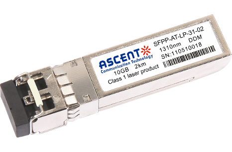
10G SFP+ LR 1310 nm 10 km
10G SFP+ LRM 1310 nm 2 km
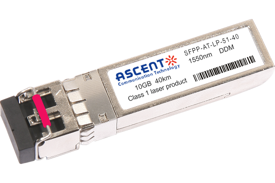
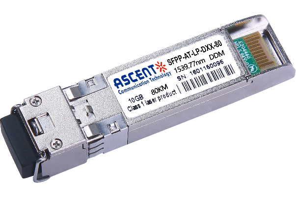
10G SFP+ ER 1550 nm 40 km
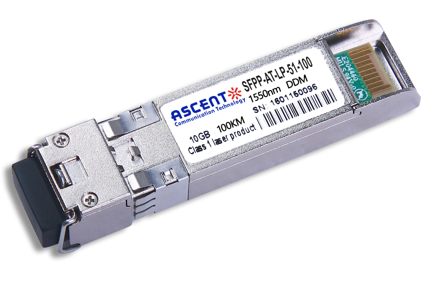
10G SFP+ CDR 1550 nm 100 km
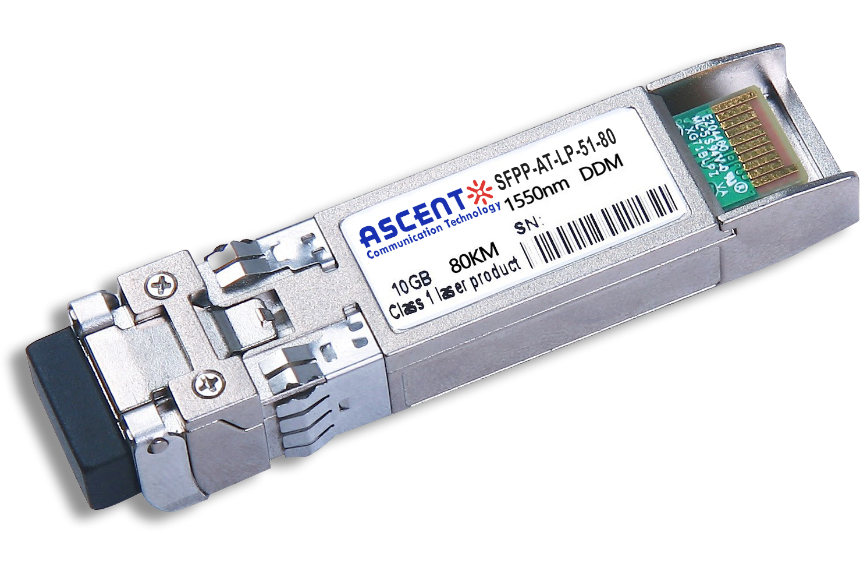
10G SFP+ ZR 1550 nm 80 km
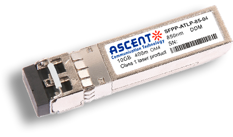
10G SFP+ 850 nm 400 m
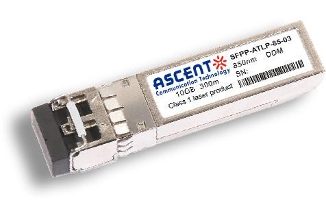
10G SFP+ 850 nm 300 m
10G SFP+ Tunable DWDM 80 km
10G SFP+ DWDM 80 km
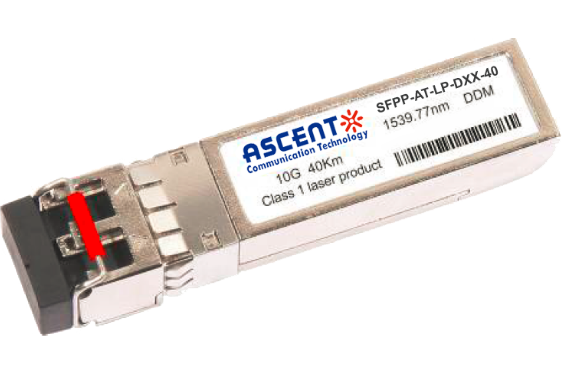
10G SFP+ DWDM 40 km

10G SFP+ CWDM 80 km
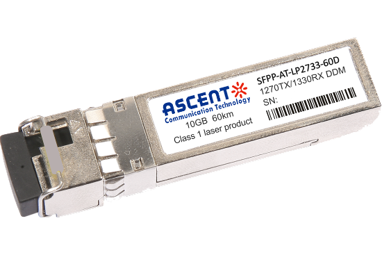
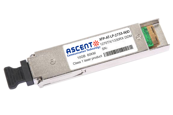
10G SFP+ CWDM 2733 60 km
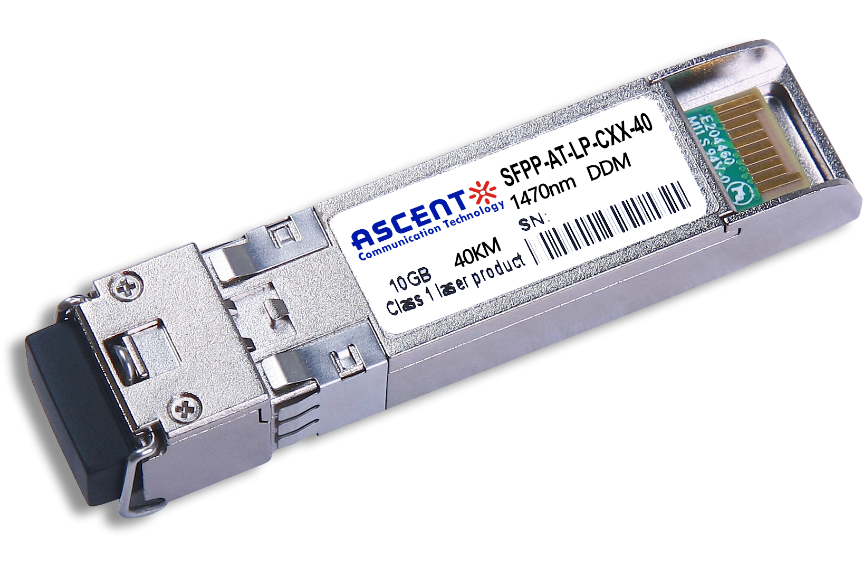
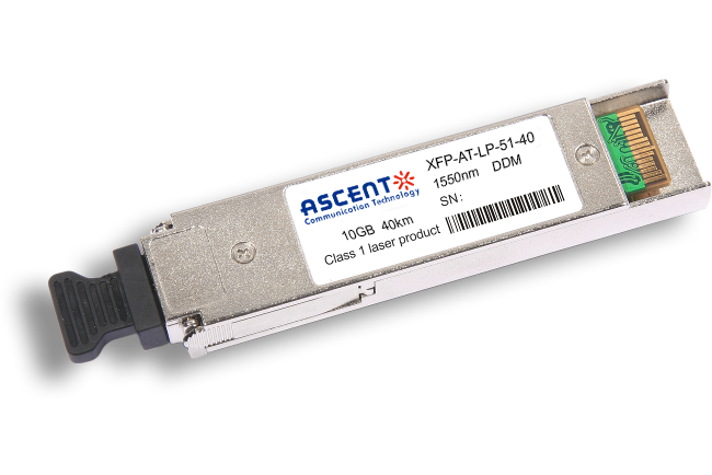
10G SFP+ CWDM 40 km
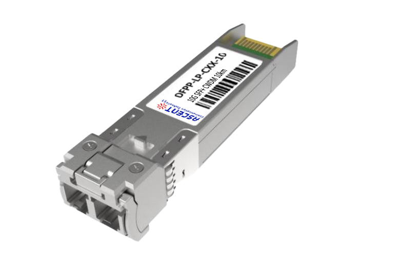
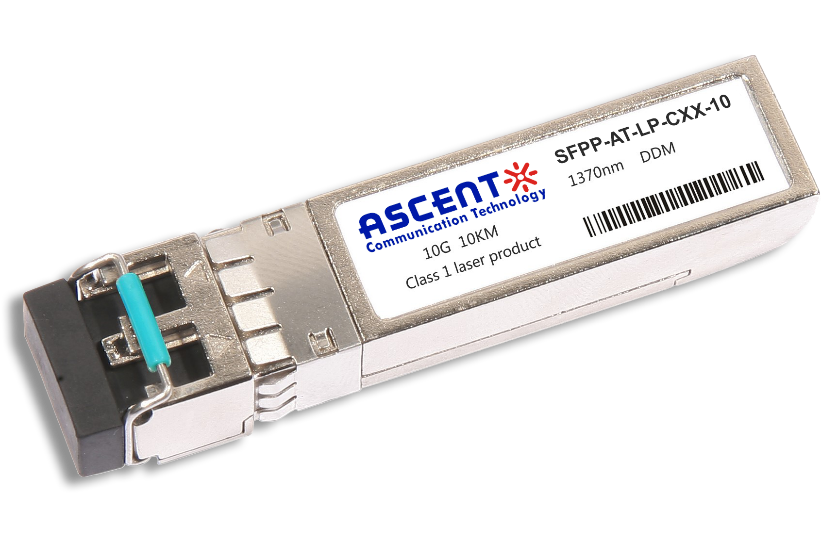
10G SFP+ CWDM 10 km
10G SFP+ Single mode CWDM 10 km
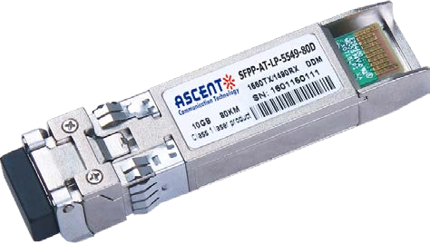
10G SFP+ CWDM 4955 80 km
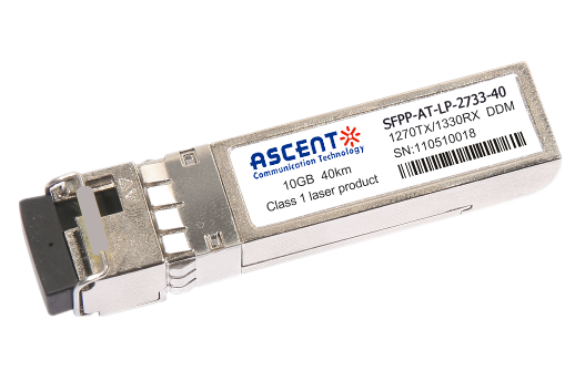
10G SFP+ CWDM 2733 40 km
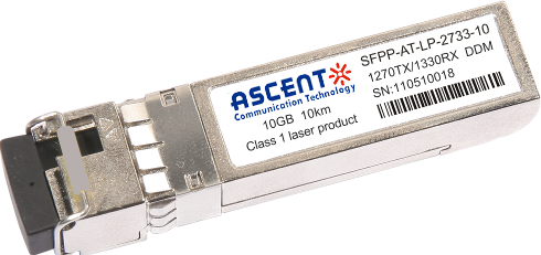
10G SFP+ CWDM 2733 10 km

10G XFP BIDI 80KM

10G XFP BIDI 40KM

10G XFP BIDI 10KM

10G XFP LR 1310 nm 20 km

10G XFP LR 1310 nm 10 km
10G XFP ER 1550 nm 40 km

10G XFP ZR 1550 nm 80 km
10G XFP CWDM 2633 60 km
10G SFP+ CWDM 1610 80 km
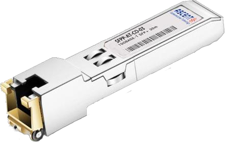
10G SFP+ Copper RJ45 30 m

10G X2 850nm 300m
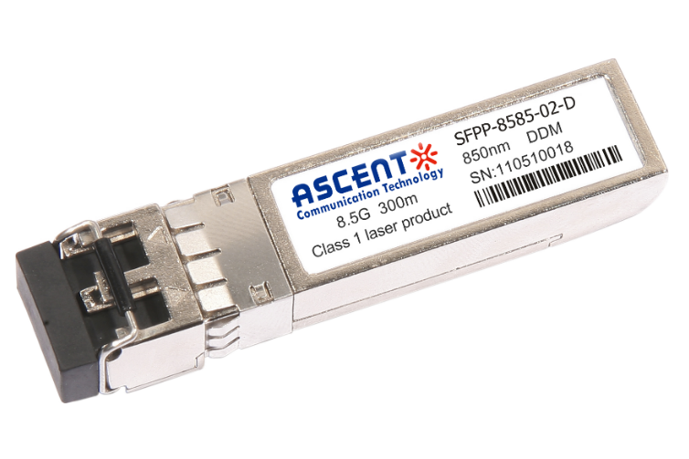
16G SFP+ FC 850 nm 100 m
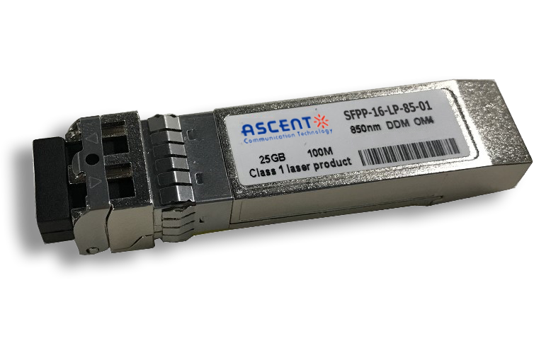
8.5G SFP+ SR 850 nm 150 m
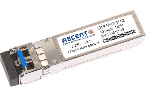
6.25G SFP+ LRM 1330 nm 2 km
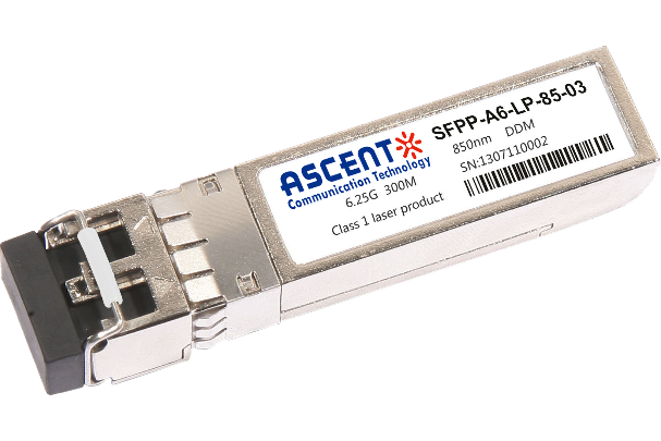
6.25G SFP+ SR 850 nm 300 m