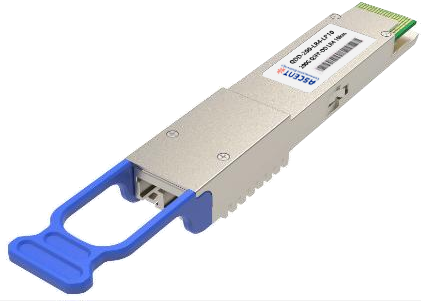
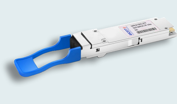
Ascent’s QSFP28 100G SR BIDI is a parallel Quad Small Form-factor Pluggable (QSFP28) Bi-Direction optical module which can support 100Gb/s bit rates in an optical communication application compliant to SFF-8636, IEEE802.3bm standards. The module integrates four host electrical data into two optical lanes (by Dual Wavelength VCSEL Bi-Directional Optical Interface, 850nm and 900nm) to allow optical communication over a 2-fiber duplex LC optical multi-mode fiber. Reversely, on the receiver side, the module de-multiplexes 2 sets of optical input signal and converts them to 4 channels of electrical data. An optical fiber ribbon cable with an LC connector can be plugged into the QSFP28 module receptacle. Proper alignment is ensured by the guide pins inside the receptacle. The cable usually cannot be twisted for proper channel to channel alignment. Electrical connection is achieved through an MSA-compliant 38-pin edge type connector. The product is designed with form factor, optical/electrical connection, and digital diagnostic interface according to the QSFP+ Multi-Source Agreement (MSA). It has been designed to meet the harshest external operating conditions including temperature, humidity, and EMI interference.
· QSFP28 MSA Specification Compliant, including new functions per SFF-8636
· 100G Link Distances up to 70m over OM3,100m over OM4
· Hot Pluggable
· Dual Wavelength VCSEL Bi-Directional Optical Interface, PAM4 2x50Gbps 850nm/908nm
· Interface with Digital monitoring and maskable Interrupts for Ex-panded functionality
· Case Operating Temperature:
Range: 0 to 70°C
· RoHS II Compliance
· Operating Mode
Parameter | Symbol | Min. | Max. | Unit | Notes |
Storage Ambient Temperature | Tstg | -40 | +85 | °C | |
Relative Humidity - Storage | RHS | 0 | 95 | % | |
Relative Humidity - Operating | RHO | 0 | 85 | % | |
Module Supply Voltage | VCC | -0.5 | 3.6 | V |
Notes:
1. Exceeding the Absolute Maximum Ratings may cause irreversible damage to the device. The device is not intended to be operated under the condition of simulta-neous Absolute Maximum Ratings, a condition which may
cause irreversible damage to the device. RH is Non-condensing condition.
Parameter | Symbol | Min. | Typ. | Max. | Unit | Notes |
Case Operating Temperature | Tcase | 0 | +25 | +70 | °C | |
Module Supply Voltage | VCC | 3.135 | 3.3 | 3.465 | V | |
Signaling Speed Per Electrical Channel(4x25G NRZ) | S | - | 25.78 | - | Gb/s | |
Power Consumption | P | - | - | 4 | W |
Parameter | Symbol | Min. | Typ. | Max. | Unit | Notes |
Transmitter | ||||||
Tx_Data Differential Input Voltage | VIN | 200 | - | 900 | mV | |
Tx_Data Differential Input Impedance | ZIN | - | 100 | - | Ω | |
Receiver | ||||||
Rx_Data Differential Output Voltage | VOUT | - | - | 1200 | mV | |
Rx_Data Differential Output Impedance | ZOUT | - | 100 | - | Ω | |
Timing Requirement of Control and Status I/O | ||||||
Tx Squelch Deassert Time | toff_Txsq | - | - | 1 | s | |
Rx Squelch Deassert Time | toff_Rxsq | - | - | 2 | s | |
Non-Volatile Memory Specification | ||||||
Complete Single or Sequential Write | twr | - | - | 80 | ms | |
Soft Control and Status Timing Requirements | ||||||
Application or Rate Select Change Time | t_ratesel | - | - | 600 | ms | |
Parameter Transmitter | Symbol
| Test Point | Min.
| Typ.
| Max.
| Unit | Notes
|
Average Launch Power ,each Lane | POUT | TP2 | -6.2 | - | 4 | dBm | Average Optical Output |
Optical modulation Amplitude , each Lane | OMA | TP2 | -4.2 | - | 3 | dBm | |
Extinction Ratio | ER | TP2 | 3 | - | - | dB | |
Launch power in OMAouter Minus TDECQ, each Lane | OMA- TDECQ | TP2 | -5.9 | - | - | dB | |
Optical Output with Tx OFF | POFF | TP2 | - | - | -30 | dBm | |
Center Wavelength 1 | λ | TP2 | 844 | 850 | 863 | nm | |
Center Wavelength 2 | λ | TP2 | 900 | 908 | 918 | nm | |
RMS Spectral Width1 | Δλ | TP2 | - | - | 0.6 | nm | |
RMS Spectral Width2 | Δλ | TP2 | - | - | 0.65 | nm | |
Optical Return Loss Tolerance | ORL | TP2 | - | - | 12 | dB | |
Transmitter and Dispersion Eye Closure for PAM4 (TDECQ), each Lane |
TDECQ |
TP2 |
4.9 |
dB | |||
Receiver | |||||||
Average Power at Receive Input, each Lane | PIN | TP3 | -7.9 | - | 4 | dBm | Note1 |
Receive Power, each Lane (OMAouter) | PIN(OMA) | TP3 | -5.9 | - | 3 | dBm | |
Unstressed Receiver Sensitivity (OMAouter), each Lane | Sen | TP3 | - | - | max(-6.6, SECQ - 8) | dBm | Note2 |
Center Wavelength1 | λ | TP3 | 844 | 850 | 863 | nm | |
Center Wavelength2 | λ | TP3 | 900 | 908 | 918 | nm | |
Receiver Reflectance | RFL | TP3 | - | - | -12 | dB | |
Rx_LOS of Signal - Assert | PA | TP3 | -30 | - | - | dBm | |
Rx_LOS of Signal - Deassert | PD | TP3 | - | - | -5.9 | dBm | |
Rx_LOS of Signal - Hysteresis | PHy | TP3 | 0.5 | - | - | dB |
Notes:
1. A received power below this value cannot be compliant; however, avalue above this does not ensure compliance.
2. Sensitivity where the BER=2.4*10-4 measured with a PRBS 31Q test pattern@26.56GBaud.


200G QSFP DD LR4 10km
200G QSFP56 SR4 850 nm 100 m

100G QSFP28 LX4 2km

100G QSFP28OA LR4 10km

100G QSFP28 ZR4 1310 nm 80 km

100G QSFP28 ER4L 1310 nm 40 km
100G QSFP28 ER4 1310 nm 40 km
100G QSFP28 LR4 1310 nm 10 km
100G QSFP28 LR Single λ 10 km

100G QSFP28 DR Single λ 500 m
100G QSFP28 CWDM4 1310 nm 2 km
100G QSFP28 PSM4 1310 nm 2 km
100G QSFP28 SR4 850 nm 100 m

100G QSFP28 FR Single λ 1310 nm 2 km

100G QSFP28 BIDI 80km

100G QSFP28 BIDI 40km

100G QSFP28 EZR4 100km

100G SFP56 ER1 30km

100G SFP56 LR1 10km
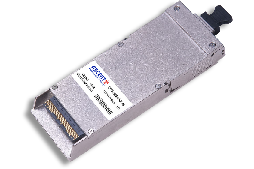
100G CFP2 ER4 40 km
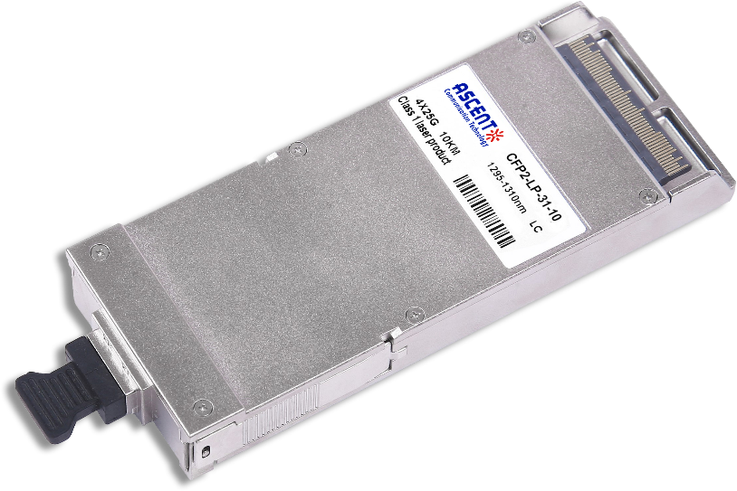
100G CFP2 LR4 10 km
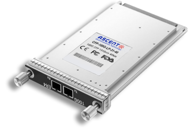
100G CFP ER4 40 km
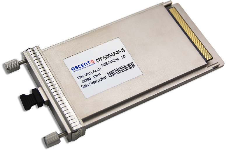
100G CFP LR4 10 km