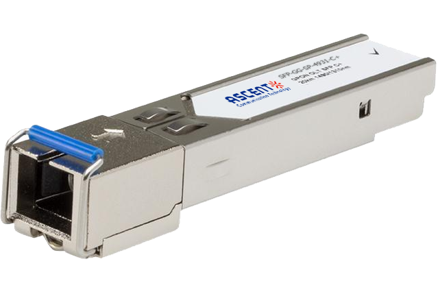
ASCENT’s GPON OLT transceiver SFP-GG-SP-4931 D+ is designed for optical line terminal (OLT) for ITU-T G.984.2 Class D+ requirements Network transmission. The optical transceiver is compliant with the Small Form- Factor Pluggable (SFP) Multi-Source Agreement (MSA). The GPON OLT SFP module is contained in a SFP package with SC/UPC receptacle connector. The module consists of 1490nm DFB laser, InGaAs APD, Preamplifier and WDM filter in a high-integrated optical sub-assembly, and it transmits up to 2.5Gbps of continuous data at 1490nm and receives 1.25Gbps burst-mode data at 1310nm. The module data links up to 20km in 9/125um single mode fiber. Ascent GPON SFP is a low-cost point to multi point (P2MP) Fiber to the Home, Business or Curb (FTTX) GPON OLT transceiver. It is fabricated with a rugged die cast metal housing and cage assembly. Commercial and industrial temperature ranges are available. It is IEC 60825-1 Class I laser safety compliant and meets the EEC Directive 2002/95/EC for RoHS compliance.
· ITU-T G.984.2 GPON OLT D+
· Bi-directional 2.5Gbps Tx and 1.25Gbps Rx
· 1490nm continuous-mode transmitter with DFB LD
· 1310nm burst-mode receiver with APD-TIA
· Digital diagnostic monitoring
· SFP package with SC/UPC receptacle optical interface
· Single +3.3V power supply
· Operation case temperature
-40 to 85°C
· RoHS6 compliance
Absolute Maximum Ratings
Parameter | Symbol | Min. | Max. | Unit | Note
|
Storage Temperature | TstG | -40 | 85 | °C | |
Operating Case Temperature | Tc | 0 | 70 | °C | |
Operating Humidity | OH | 5 | 95 | % | |
Power Supply Voltage | VCC | 0 | 3.6 | V | |
Receiver Damage Threshold | +5 | dBm |
Recommended Operating Conditions
Parameter | Symbol | Min. | Typ. | Max. | Unit | Note |
Power Supply Voltage | VCC | 3.13 | 3.3 | 3.47 | V | |
Power Supply Current | 350 | 500 | mA | |||
Operating Case Temperature | Tc | 0 | 70 | °C | ||
Operating Humidity Range | OHo | 5 | 85 | % | ||
Nominal Data Rate | Tx 1244.16 Rx 2488.32 | Mbit/s |
Parameter | Symbol | Min. | Typ. | Max. | Unit | Note |
Optical Center Wavelength | 1480 | 1500 | nm | |||
Optical Spectrum Width (-20dB) | ∆λ | 1 | nm | |||
Side Mode Suppression Ratio | SMSR | 30 | dB | |||
Average Launch Optical Power | AOP | +6 | +10 | dBm | EOL, 0~70°C | |
Power-OFF Transmitter Optical Power | -39 | dBm | Launched into SMF | |||
Extinction Ratio | ER | 8.2 | dB | PRBS223-1+72CID @2.488Gbit/s | ||
Tolerance to Transmitter Incident Light | -15 | dB | ||||
Transmitter Reflectance | -10 | dB | ||||
Transmitter and Dispersion Penalty | TDP | 1 | dB | Transmit on 20km SMF | ||
Optical Waveform Diagram | ITU-T G.984.2 | Figure 1,margin>5% | ||||
Output Eye Mask | Compliant with ITU5T G.984.2 Mask | |||||
Transmitter Electrical Characteristics
Parameter | Symbol | Min. | Typ. | Max. | Unit | Note |
Data Input Differential Swing | 600 | 1600 | mV | LVPECL input, AC coupled | ||
Input Differential Impedance | 90 | 100 | 110 | Ω | ||
Transmitter Disable Voltage - Low | 0 | 0.8 | V | |||
Transmitter Disable Voltage - High | 2.0 | VCC | V | |||
Transmitter Fault Alarm Voltage - Low | 0 | 0.4 | V | |||
Transmitter Fault Alarm Voltage - High | 2.4 | VCC | V |

Transmitter Eye Mask Definitions and Test Procedure
Parameter | Symbol | Min. | Typ. | Max. | Unit | Note |
Operating Wavelength | SEN | 1290 | 1330 | nm | ||
Sensitivity (EOL, 0~70°C) | -35 | dBm | PRBS223- 1+72CID@1.244Gbps BER ≤1×10⁻⁴ ,ER≥10dB | |||
Saturation Optical Power | dBm | |||||
Dynamic Range | 15 | dB | Figure 2 | |||
SD Signal Assert Level | -36 | dBm | ||||
SD Signal De-assert Level | -45 | dBm | ||||
Hysteresis | 0.5 | 6 | dB | |||
Receiver Reflectance | 12 | dB |

Burst Mode Receiver Dynamic Range in GPON System
Receiver Electrical Characteristics
Parameter | Symbol | Min. | Typ. | Max. | Unit | Note |
Data Output Voltage – Low | Vcc-1.81 | Vcc-1.62 | V | |||
Data Output Voltage – High(-Vcc) | Vcc-1.02 | Vcc-0.88 | V | |||
Data Output Differential Swing | 400 | 1600 | mV | LVPECL output, DC coupled | ||
Reset with | TRESET | 16 | bits | |||
Reset-Low | 0 | 0.4 | V | |||
Reset- High | 2.4 | Vcc | V | |||
Receiver Amplitude Recovery | TRECOVERY | 32 | bits | Refer to the Reset signal falling | ||
Signal Detect Assert Time | 50 | ns | ||||
Signal Detect De-assert Time | 12.8 | ns | Refer to the Reset signal rising | |||
Signal Detect Voltage-Low | 0 | 0.4 | V | |||
Signal Detect Voltage- High | 2.4 | Vcc | V | |||
RSSI Trigger-Low | 0 | 0.8 | V | |||
RSSI Trigger- High | 2.0 | Vcc | V | |||
Optical Signal During Time | Tont | 1200 | ns | |||
RSSI Trigger- High | 2.0 | Vcc | V | |||
Optical Signal During Time | Tont | 1200 | ns |
Digital Diagnostic Monitoring
Parameter | Range | Accuracy | Calibration | Note |
Temperature | 0 to +70 °C | ±3°C | Internal | 1LSB = 1/256°C |
Voltage | 3.0 to 3.7 V | ±3% | Internal | 1LSB = 0.1mV |
Bias Current | 0 to 100 mA | ±10% | Internal | 1LSB = 2uA |
TX Power | 1.5 to 5 dBm | ±2dB | Internal | 1LSB = 0.1uW |
RX Power Monitor | -30 to -8 dBm | ±3dB | External | 1LSB = 0.1uW |
Note: The digital diagnostic monitoring interface defines 256-byte memory map in EEPROM, which makes use of the 8 bit address 1010001X(A2h).

Mechanical Dimensions
Timing Parameter Definitions in Burst More Sequence
RSSI TIMING SEQUENCE
SFP Network
SFP Pin (Golden Finger) Drawing
Typical Interface Circuit